Introduction
The journey from a circuit design concept to a functional electronic product is often fraught with potential pitfalls. For engineers and designers, the prototyping phase of printed circuit board (PCB) assembly is a critical juncture where many of these challenges surface. As an assembly engineer, I consistently advocate for the proactive application of Design for Manufacturability (DFM) guidelines. Implementing DFM early in the prototype stage is not merely a recommendation; it is a fundamental strategy for avoiding costly mistakes, accelerating development cycles, and ensuring the successful transition to mass production. This article will explore key DFM principles specifically tailored for prototype PCB assembly.
What is Design for Manufacturability (DFM) and Why It Matters for Prototypes
Design for Manufacturability (DFM) is an engineering methodology that focuses on designing products in a way that makes them easy to manufacture. In the context of PCB assembly, DFM involves optimizing the PCB layout and component selection to streamline the manufacturing and assembly processes, reduce costs, and improve overall product quality.
For prototype PCB assembly, DFM is exceptionally critical. Prototypes are often produced in small batches, and discovering manufacturing issues at this stage can be particularly disruptive and expensive. A poorly designed prototype can lead to:
- Assembly failures: Components not fitting, solder shorts, or opens.
- Rework: Extensive manual correction, consuming time and labor.
- Schedule delays: Pushing back testing and validation phases.
- Increased costs: Due to material waste, additional labor, and repeated fabrication runs.
By integrating DFM guidelines early, designers can identify and mitigate potential manufacturing problems before the first board is even fabricated. This proactive approach ensures that the prototype is not only functionally correct but also ready for efficient and high-yield assembly, laying a solid foundation for future production scale-up. It shifts the focus from merely "making it work" to "making it manufacturable."
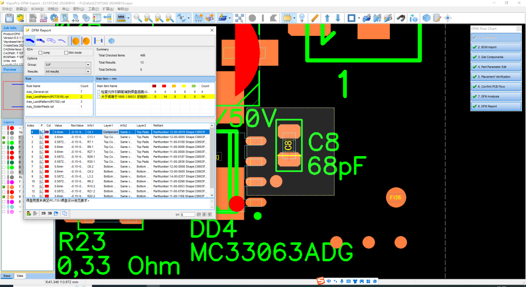
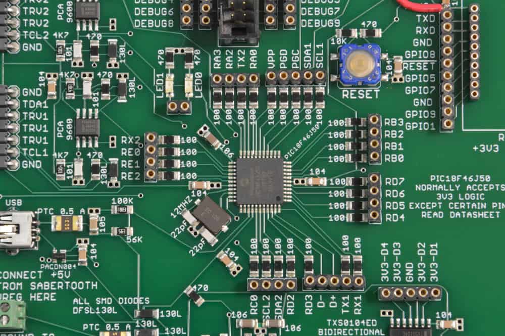
Key DFM Guideline: PCB Layout Review for Manufacturability
A comprehensive PCB layout review is a cornerstone of effective design for manufacturability (DFM) for prototype PCB assembly. This review extends beyond electrical correctness to scrutinize how the physical design impacts every stage of manufacturing and assembly.
During the PCB layout review, several critical aspects must be examined:
- Trace Widths and Spacing: Ensure that trace widths are appropriate for current carrying capacity and that spacing between traces, pads, and planes meets the capabilities of the chosen PCB manufacturer. Violations can lead to shorts or opens during fabrication. Standards like IPC-2221B, "Generic Standard on Printed Board Design," provide detailed guidance on these parameters.
- Annular Rings: Verify that annular rings (the copper ring around a drilled hole) are adequate for reliable connections to vias and through-hole component leads. Insufficient annular rings can lead to "breakout" during drilling, compromising PTH reliability.
- Solder Mask and Solder Paste Design: The solder mask must provide sufficient isolation between pads to prevent solder bridges. The solder paste stencil design (aperture size, shape, and thickness) needs to be optimized for proper paste deposition, ensuring good solder joint formation without excessive paste or insufficient volume. Misalignment or improper sizing can cause shorts or opens, particularly with fine pitch components.
- Panelization: For small boards or high-volume prototypes, consider panelization during the layout stage. This involves arranging multiple PCBs on a larger panel for efficient manufacturing and assembly. The panel design must include proper break-away tabs, fiducials, and tool holes.
- Copper Weight and Finish: Confirm that the specified copper weight and surface finish (e.g., ENIG, HASL) are appropriate for the application and compatible with the assembly processes.
A thorough PCB layout review catches these issues early, preventing costly re-spins and ensuring that the prototype can be assembled efficiently.
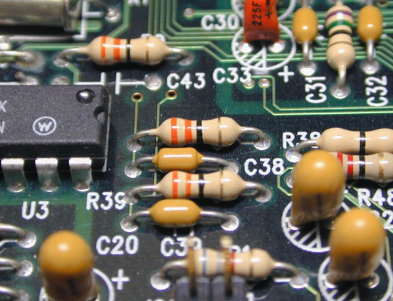
Optimizing Assembly: Component Placement Guidelines
Effective component placement guidelines are fundamental to achieving high-yield prototype PCB assembly. Thoughtful placement minimizes assembly errors, facilitates inspection, and optimizes soldering processes.
- Spacing and Clearance: Ensure adequate spacing between components, especially between large components and smaller, delicate ones. This allows for proper tool access during automated pick-and-place, prevents interference, and facilitates rework. Minimum clearances between components and the board edge are also crucial for manufacturing processes.
- Orientation: Consistent orientation of polarized components (diodes, electrolytic capacitors, ICs) in the same direction across the board can reduce setup time for pick-and-place machines and minimize errors. Marking pin 1 or polarity indicators clearly on the silkscreen is essential.
- Fiducial Marks: Include global and local fiducial marks on the PCB layout. These are copper pads used by automated assembly equipment (pick-and-place, AOI) for precise alignment. Placement should follow IPC-7351B, "Generic Requirements for Surface Mount Design and Land Pattern Standard."
- Component Grouping: Group similar components together where possible to optimize feeder setup on pick-and-place machines. Also, group components for functional blocks to simplify debugging.
- Accessibility for Rework and Inspection: Arrange components to allow access for inspection tools (e.g., AOI cameras) and rework equipment (e.g., soldering irons, hot air stations). Avoid placing tiny components directly next to large components that might block access.
- Minimize Component Overlap: Avoid overlapping components, especially on opposing sides of the board, to prevent interference during assembly and soldering processes like reflow.
Adhering to these component placement guidelines during the initial design phase ensures that the prototype PCB assembly process is as smooth and error-free as possible, saving valuable time and resources.
Critical Considerations for Prototypes: Impedance Control and Thermal Management
For many modern PCB designs, particularly those involving high-speed signals or significant power dissipation, critical considerations like impedance control in prototypes and thermal management in PCB design are paramount DFM guidelines. These aspects, if neglected, can lead to severe functional failures even in prototypes.
Impedance Control in Prototypes
High-speed digital signals and RF circuits require traces to have a specific characteristic impedance to prevent signal reflections, which can degrade signal integrity and cause functional issues. Achieving accurate impedance control in prototypes involves:
- Trace Geometry: Precisely defining trace width, height, and the distance to reference planes.
- Dielectric Material: Using a consistent and known dielectric constant (Er) of the PCB laminate material.
- Stack-up Definition: Clearly specifying the PCB stack-up (layer order, material thickness) to the manufacturer.
Even slight variations in these parameters can alter impedance. It is crucial to communicate these impedance requirements clearly to the PCB fabricator during the quotation and fabrication stages. For prototypes, simulating impedance using field solvers and verifying with time-domain reflectometry (TDR) measurements can confirm the design's integrity. IPC-2221B provides general guidelines for trace routing that support impedance control.
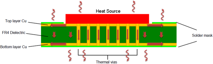
Thermal Management in PCB Design
Effective thermal management in PCB design is essential to prevent components from overheating, which can lead to reduced performance, premature failure, or even catastrophic damage. For prototypes, where the final thermal profile might not be fully understood, proactive DFM for thermal aspects is vital:
- Component Placement: Placing heat-generating components away from heat-sensitive ones.
- Thermal Vias: Incorporating thermal vias (plated through-holes used for heat transfer) under power components to conduct heat to ground planes or other layers.
- Copper Planes: Utilizing large copper planes (power and ground planes) to act as heat sinks and spreaders.
- Trace Widths: Using wider traces for power lines to reduce I2R losses and subsequent heat generation.
Simulating the thermal performance of the PCB layout can help identify potential hot spots early. Ignoring thermal management in prototype PCB design can lead to unreliable operation and necessitate costly redesigns later.
Benefits of Applying DFM Early in Prototype Development
The proactive application of DFM guidelines during prototype development yields a multitude of benefits, translating directly into a more efficient and successful product development cycle.
- Reduced Costs: By identifying and resolving manufacturing issues at the design stage, significant costs associated with rework, scrap materials, and repeat fabrication runs are avoided. A well-designed prototype is cheaper and faster to build correctly the first time.
- Faster Time to Market: Eliminating manufacturing hurdles early on streamlines the prototyping and assembly phases. This accelerates the validation process, allowing the product to move from development to market launch much more quickly.
- Improved Product Quality and Reliability: Designs that are inherently manufacturable tend to be more robust. DFM helps ensure consistent quality in every assembled board, leading to higher product reliability and fewer field failures. This aligns with quality management principles found in ISO 9001:2015, "Quality Management Systems."
- Enhanced Communication and Collaboration: DFM promotes better communication between design, manufacturing, and assembly teams. Early involvement of assembly engineers and manufacturing specialists ensures that practical production considerations are integrated into the design, fostering a collaborative environment.
- Smoother Transition to Mass Production: A prototype that has been designed with DFM in mind is inherently easier to scale for mass production. The manufacturing processes established for the prototype can be readily optimized and replicated for higher volumes, minimizing surprises and maintaining consistent quality.
Ultimately, DFM is not just about making a product, but about making a better product, more efficiently and reliably, especially starting from the critical prototype phase.
Conclusion
The successful development of electronic products hinges on robust design practices, and for prototype PCB assembly, Design for Manufacturability (DFM) is paramount. By diligently adhering to DFM guidelines through a meticulous PCB layout review, optimizing component placement guidelines, and critically addressing aspects like impedance control in prototypes and thermal management in PCB design, engineers can preempt a multitude of costly mistakes. This proactive approach not only streamlines the prototyping process but also lays a strong foundation for future mass production, leading to reduced costs, faster time to market, and ultimately, higher quality and more reliable electronic products.
FAQs
Q1: What is Design for Manufacturability (DFM) in the context of prototype PCB assembly?
A1: Design for Manufacturability (DFM) in prototype PCB assembly is the practice of designing the PCB layout and selecting components to optimize for ease, efficiency, and cost-effectiveness of manufacturing and assembly. It aims to identify and resolve potential production issues early, preventing costly mistakes and delays in the prototyping phase.
Q2: Why is a thorough PCB layout review crucial for DFM in prototypes?
A2: A thorough PCB layout review is crucial for DFM in prototypes because it ensures the design complies with manufacturing capabilities and standards. It helps verify critical aspects like trace widths, spacing, annular rings, and solder mask design, which directly impact the yield and reliability of the PCB assembly process.
Q3: What are key component placement guidelines for efficient prototype PCB assembly?
A3: Key component placement guidelines for efficient prototype PCB assembly include ensuring adequate spacing and clearance, consistent orientation of polarized components, incorporating fiducial marks for automated assembly, grouping similar components, and allowing accessibility for inspection and rework. These practices streamline the assembly process and reduce errors.
Q4: How do impedance control and thermal management contribute to DFM for prototypes?
A4: Impedance control in prototypes is vital for maintaining signal integrity in high-speed circuits by ensuring traces have specific characteristic impedances. Thermal management in PCB design prevents overheating by strategically placing components, utilizing thermal vias, and designing copper planes for heat dissipation. Both are critical DFM aspects to ensure prototype functionality and reliability.
References
IPC-A-610G — Acceptability of Electronic Assemblies. IPC, 2017.
IPC-2221B — Generic Standard on Printed Board Design. IPC, 2012.
IPC-7351B — Generic Requirements for Surface Mount Design and Land Pattern Standard. IPC, 2010.
J-STD-001G — Requirements for Soldered Electrical and Electronic Assemblies. IPC/JEDEC, 2017.
ISO 9001:2015 — Quality Management Systems. ISO, 2015.