Introduction
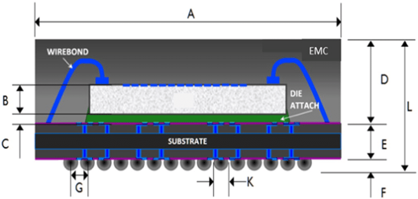
Ball Grid Array (BGA) components represent a cornerstone in modern electronics assembly, enabling high-density interconnections on printed circuit boards. These packages feature an array of solder balls beneath the component, which form critical electrical and mechanical joints during reflow soldering. However, the hidden nature of these joints beneath the package body poses significant challenges for quality assurance in manufacturing environments. Traditional optical inspection methods fall short, as they cannot penetrate the component to reveal internal defects. This is where BGA x-ray inspection emerges as an indispensable tool, providing non-destructive visibility into solder joint integrity. By leveraging X-ray technology, factories can detect issues like voids and misalignment early, ensuring long-term reliability in demanding applications such as telecommunications and computing hardware.
The adoption of BGA x-ray inspection has become standard in high-volume production lines to meet the expectations of electric engineers focused on robust assembly processes. Defects in BGA solder joints can lead to intermittent failures, thermal management problems, or complete circuit breakdowns under operational stress. X-ray systems allow for real-time or post-process evaluation, aligning with factory-driven quality control protocols. As PCB densities increase, the precision of x-ray inspection for BGA solder joints directly impacts yield rates and product lifespan. This article explores the technical underpinnings, defect detection capabilities, and practical implementation of BGA x-ray inspection, demystifying its role in achieving dependable assemblies.
What Is BGA X-Ray Inspection and Why It Matters
BGA x-ray inspection involves directing a beam of X-rays through the assembled board to produce radiographic images of the solder joints. The varying densities of materials, such as solder versus air or substrate, create contrast in these images, highlighting potential anomalies. This technique is particularly vital for BGAs because the solder balls are inaccessible from the top or bottom without destructive sectioning. Factories rely on it to verify joint formation after reflow, where processes like vapor phase or convection heating can introduce variability. Without such inspection, latent defects could propagate to field failures, escalating costs and damaging reputation.
The relevance of x-ray inspection for BGA solder joints stems from the scale and complexity of modern assemblies. BGA packages often feature hundreds of fine-pitch balls, amplifying the risk of process-induced flaws. Electric engineers prioritize this method because it supports data-driven process optimization, such as stencil aperture adjustments or profile refinements. In high-reliability sectors, undetected issues compromise signal integrity and thermal dissipation, leading to performance degradation. Ultimately, integrating BGA x-ray inspection into the production workflow safeguards against these risks, fostering consistent quality across batches.
Principles of X-Ray Technology in BGA Inspection
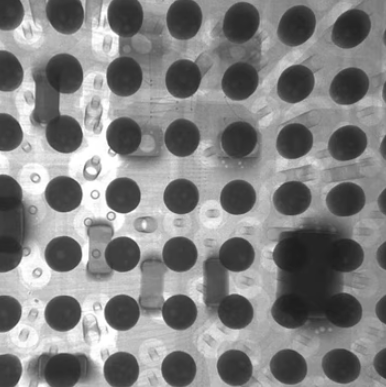
X-ray inspection operates on the principle of differential absorption, where X-rays pass through the PCB assembly and are attenuated differently by materials of varying atomic density. Solder, being lead-tin alloy, appears dark on the radiograph due to higher absorption, while voids or gaps manifest as brighter regions. Systems typically employ a microfocus X-ray source to achieve high resolution, often down to microns, essential for fine-pitch BGAs. Oblique-angle imaging enhances visibility by reducing superposition from overlapping balls, allowing clearer differentiation of joint shapes. Factories configure these systems for 2D transmission, 2.5D laminography, or full 3D computed tomography based on inspection depth requirements.
In practice, the X-ray beam geometry plays a crucial role in accurate BGA evaluation. Tilt mechanisms enable angled views that reveal fillet formation and ball standoff, which are obscured in straight-on projections. Image processing software enhances contrast and applies edge detection to quantify features like ball diameter uniformity. This non-contact method preserves component integrity, making it ideal for both inline monitoring and rework verification. Electric engineers appreciate how these principles translate to quantifiable metrics, supporting statistical process control in manufacturing.
Key Defects Detected by BGA X-Ray Inspection
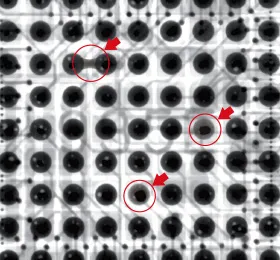
BGA void detection stands out as a primary application of x-ray inspection, where gas entrapment during reflow creates air pockets within the solder bulk. These voids appear as low-density spots on radiographs, potentially compromising electrical conductivity and heat transfer. Excessive voiding correlates with flux residue or rapid heating rates, prompting process tweaks like nitrogen atmospheres. X-ray systems quantify void distribution across the array, identifying peripheral versus central patterns that inform root cause analysis. In factory settings, routine scans flag assemblies exceeding acceptable thresholds, preventing shipment of unreliable boards.
Misalignment in BGA placement manifests as offset solder balls, where the component shifts relative to pad centers during reflow. X-ray images reveal this through asymmetric joint shadows or incomplete wetting on one side. Causes include poor stencil printing or board warpage, both detectable via complementary metrology. Correcting misalignment early avoids stress concentrations that accelerate fatigue. Beyond voids and BGA misalignment, x-ray uncovers bridging between adjacent balls, non-wet opens, and head-in-pillow defects, where the solder ball fails to fully merge with the pad solder paste.
Other defects like insufficient solder volume show as undersized joints, while cracks appear as linear discontinuities. These insights enable targeted troubleshooting, such as paste release optimization. Electric engineers use these defect signatures to refine design rules, ensuring pad-to-ball ratios support robust merging.
X-Ray Inspection Standards for BGA Solder Joints
Industry standards provide the framework for interpreting BGA x-ray inspection results, with IPC J-STD-001 recommending X-ray as a verification method for hidden solder joints. This standard outlines soldering requirements that encompass joint fillet visibility and void limits through radiographic evaluation. Factories align their criteria to these guidelines to ensure consistency across suppliers and processes. IPC-A-610 further defines acceptability classes, specifying characteristics observable via X-ray, such as ball offset tolerances and void aggregation.
IPC-7095 offers BGA-specific guidance on design and assembly implementation, including inspection techniques for voiding and misalignment. It emphasizes process controls that minimize defects detectable by X-ray, promoting reliable implementation in high-density boards. These standards collectively drive factory protocols, from operator certification to equipment calibration. Adherence reduces variability, supporting electric engineers in specifying compliant assemblies.
Best Practices for Implementing BGA X-Ray Inspection in Factories
Establishing a robust BGA x-ray inspection protocol begins with system selection suited to pitch sizes and volume throughput. Microfocus tubes with geometric magnification ensure resolution for 0.3 mm pitches and finer. Operators train on oblique viewing angles, typically 30 to 45 degrees, to optimize defect contrast without distortion. Integrating automated X-ray with AOI creates hybrid lines, where optical pre-screens direct detailed radiographic checks. Sampling strategies, such as AQL plans, balance coverage with efficiency, inspecting full arrays on first articles and statistical subsets thereafter.
Process integration involves linking x-ray data to upstream metrics like reflow profiles and paste inspection. Regular calibration against phantoms verifies accuracy, while software algorithms automate void percentage calculations. Factories document thresholds per class, escalating outliers for sectioning verification. This closed-loop approach refines yields, minimizing escapes.
Troubleshooting common challenges enhances effectiveness. Overlapping shadows in dense arrays demand multi-angle acquisition, while high-Z materials like copper vias require density compensation. Operator fatigue mitigation through automation ensures consistent reads. Electric engineers benefit from archived images for failure analysis, correlating defects to design features.
Challenges in BGA X-Ray Inspection and Solutions
Dense BGA arrays challenge 2D X-ray due to ball superposition, often necessitating 3D techniques for volumetric rendering. Vias beneath pads create artifacts mimicking voids, resolvable by multi-view reconstruction. Radiation exposure limits scan times, balanced by high-flux sources in enclosed cabinets. Factories mitigate these via protocol standardization, such as predefined tilt sequences.
Software advancements address quantification variability, applying machine vision for repeatable measurements. Training emphasizes standard interpretation, reducing subjective calls. These solutions elevate x-ray from qualitative to quantitative tool.
Conclusion
X-ray technology demystifies BGA inspection, offering unparalleled insight into hidden solder joints critical for reliable electronics. From void detection to misalignment assessment, it empowers factories to uphold quality amid rising complexity. Standards like IPC J-STD-001 and IPC-A-610 guide criteria, ensuring alignment with engineering expectations. Best practices in implementation yield process stability and high confidence. Electric engineers can leverage these methods for robust designs and fewer field issues. Ultimately, BGA x-ray inspection secures the foundation of advanced PCB assemblies.
FAQs
Q1: What is BGA x-ray inspection and when is it necessary?
A1: BGA x-ray inspection uses radiographic imaging to examine hidden solder joints beneath Ball Grid Array components. It becomes essential post-reflow to detect defects invisible to optical methods, particularly in high-density boards. Factories apply it for process verification and 100% inspection on critical assemblies, aligning with standards like IPC J-STD-001. This ensures joint reliability without destructive testing.
Q2: How does x-ray inspection for BGA solder joints detect voids?
A2: Voids appear as brighter, low-density regions within the darker solder mass on X-ray images due to gas pockets from reflow. BGA void detection quantifies size and distribution, flagging aggregates that impair thermal or electrical performance. Factories use oblique angles for accurate sizing, integrating results into quality gates per IPC-A-610 criteria.
Q3: What causes BGA misalignment and how is it identified via X-ray?
A3: Misalignment arises from placement errors, warpage, or reflow shear, shifting balls from pad centers. X-ray reveals offset through asymmetric wetting or standoff variations in angled views. Corrective actions include fixture improvements, with inspections confirming compliance to prevent stress failures.
Q4: What are x-ray inspection standards for BGA assemblies?
A4: Key standards include IPC-7095 for BGA-specific processes and IPC J-STD-001 for soldering verification via X-ray. These outline defect criteria like voids and BGA misalignment, guiding factory acceptability classes. They promote consistent radiographic evaluation for reliable outcomes.
References
IPC J-STD-001 — Requirements for Soldered Electrical and Electronic Assemblies. IPC.
IPC-A-610 — Acceptability of Electronic Assemblies. IPC.
IPC-7095 — Design and Assembly Process Implementation for BGAs. IPC.


