Introduction
Fine-pitch component assembly challenges electrical engineers with demands for precision and reliability in high-density electronics. Components such as ball grid arrays with pitches below 0.8 mm require substrates that maintain flatness during reflow soldering and ensure robust interconnections. Selecting the appropriate PCB substrate directly impacts yield rates and long-term performance in applications like smartphones, servers, and medical devices. Poor substrate choices lead to issues like bridging, opens, or head-in-pillow defects that compromise functionality. This article explores key substrate properties, HDI PCB integration, surface finishes, and practical strategies for successful assembly. Engineers can optimize designs by understanding how substrate characteristics align with fine-pitch BGA requirements.
Understanding Fine-Pitch BGA Substrates and Their Importance
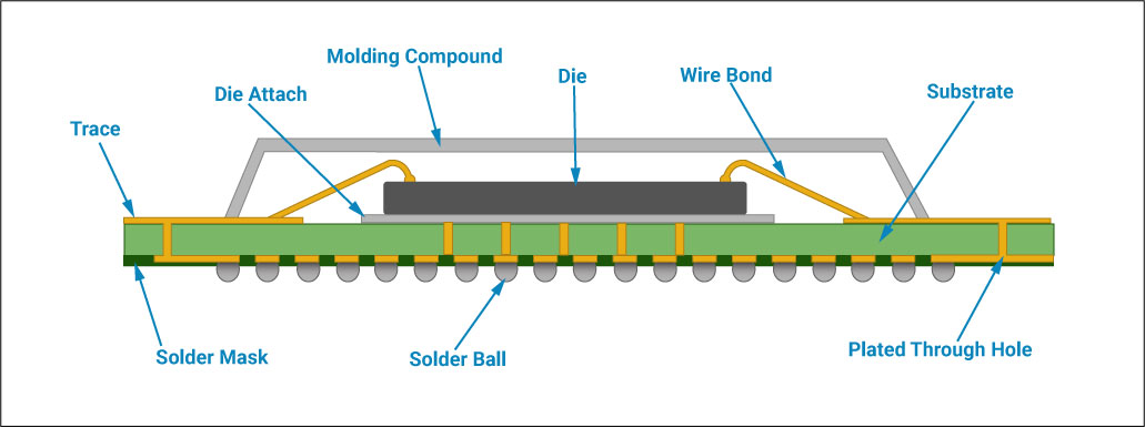
A fine pitch BGA substrate forms the foundational layer stackup that supports dense ball grid arrays with pitches typically ranging from 0.4 to 0.65 mm. These substrates must exhibit low coefficient of thermal expansion to match the silicon die and prevent stress during thermal cycling. High glass transition temperature materials resist softening at reflow peaks around 260°C, preserving planarity. Dimensional stability prevents misalignment of fine-pitch balls during placement and soldering. In production, substrates with inadequate properties cause warpage that lifts edges or bows centers, leading to inconsistent solder joints. Engineers prioritize these traits to achieve high first-pass yields in surface mount technology lines.
Substrate selection influences the entire assembly workflow from stencil printing to inspection. Thinner cores and build-up layers in advanced substrates enable tighter routing under the component footprint. Compatibility with microvia technology becomes essential for escaping signals from under the BGA. Without proper CTE matching, thermo-mechanical fatigue accelerates in field use, shortening product lifespan. Testing substrates for warpage per industry guidelines ensures predictability. Practical evaluation involves shadow moiré analysis at elevated temperatures to simulate reflow conditions.
Related Reading: Basics of routing with BGA packages
Key Material Properties for Fine-Pitch BGA Substrates
Core materials like high-Tg FR-4 variants or resin-coated copper provide the mechanical backbone for fine pitch BGA substrates. Low CTE in the Z-axis minimizes via barrel cracking under thermal stress, a common failure mode in multilayer boards. High modulus materials resist deformation, maintaining pad coplanarity for reliable ball collapse. Fillers in resins enhance rigidity while reducing moisture absorption, which exacerbates popcorn effects during soldering. Engineers specify these properties based on component datasheets and assembly profiles to avoid costly rework.
Warpage control stands out as a critical factor, with substrates engineered for symmetry in copper distribution and material thickness. Asymmetric stackups induce convex or concave bowing that misaligns fine-pitch balls by microns. Sequential build-up processes layer low-warpage dielectrics to balance stresses. IPC-7095 outlines guidelines for BGA design and assembly, emphasizing substrate flatness to support fine-pitch implementation. Troubleshooting warpage starts with vendor material data sheets and progresses to prototype testing. Consistent baking and storage protocols further stabilize substrates pre-assembly.
HDI PCB substrates incorporate advanced dielectrics for microvia drilling and plating. Laser-drilled vias with aspect ratios under 1:1 demand resin systems that plate uniformly without voids. Build-up films offer finer line widths and spaces, essential for fanout from 0.4 mm pitch BGAs. These substrates integrate core and outer layers seamlessly, supporting any-layer vias in complex designs. Electrical performance benefits from controlled impedance in microvia transitions. Reliability testing verifies via integrity through thermal cycling and bias stressing.
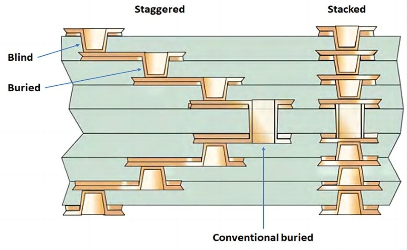
Microvia Technology in HDI PCBs for Fine-Pitch Assembly
Microvia technology revolutionizes HDI PCB substrates by enabling direct connections under fine-pitch BGAs, reducing layer count and board size. Stacked or staggered microvias drill through thin dielectrics, plated with copper to form reliable paths. Aspect ratios below 0.8 ensure complete fill and minimal stub effects for high-speed signals. Filled vias prevent solder wicking during assembly, preserving joint integrity. Engineers design via-in-pad configurations to maximize density without dogbone escapes. IPC-6012DS specifies qualification criteria for HDI structures, including microvia reliability.
Process control during microvia formation prevents reliability pitfalls like cracking at via-to-pad interfaces. Plasma cleaning removes drill smears, enhancing adhesion for plating. Sequential lamination builds multiple microvia layers without core distortion. For fine pitch BGA substrates, microvia fanout patterns route signals efficiently to inner layers. Troubleshooting involves cross-sectioning samples to inspect via fill and barrel quality. This technology proves indispensable for compact assemblies in wearables and automotive electronics.
Related Reading: Mastering Microvias: A Comprehensive Guide to HDI PCB Design
Substrate Surface Finish and Its Role in Solderability
Substrate surface finish protects exposed copper pads from oxidation while promoting wetting for fine-pitch soldering. Immersion finishes like gold over nickel deliver flat surfaces ideal for 0.5 mm pitch BGAs, minimizing shadows in stencil printing. Organic solderability preservatives offer cost-effective alternatives but require careful handling to avoid degradation. Electroless nickel immersion gold excels in multiple reflow cycles due to its barrier properties. J-STD-001 defines requirements for soldered assemblies, stressing surface finish solderability for defect-free joints. Engineers select finishes based on assembly environment and component alloy.
Solderability testing via dip-and-look or wetting balance confirms finish performance before full production. Poor finishes lead to non-wetting, de-wetting, or bridging in fine-pitch arrays. Thickness control prevents issues like black pad degradation in immersion gold. For HDI PCB substrates, finishes must accommodate microvia caps without compromising planarity. Shelf life management through vacuum packaging extends usability. Practical tip: Pair finishes with flux types optimized for the metallurgy to boost yields.
Best Practices for Selecting and Preparing Substrates
Start substrate selection by matching CTE to the BGA package, typically aiming for 12-16 ppm/°C in the XY plane. Review vendor qualification data for Tg, moisture absorption, and warpage specs aligned with assembly profiles. Prototype panels with daisy-chain nets validate solder joint reliability under accelerated life testing. Bake substrates at 125°C for four hours to remove absorbed moisture, preventing delamination. Use carrier pallets for thin panels during reflow to combat warpage. Document stackup details for repeatability across batches.
Handling protocols minimize contamination and mechanical stress on fine pitch BGA substrates. ESD-safe environments and cleanroom protocols protect surface finishes. Stencil design incorporates finer apertures for low-volume paste deposition under tight pitches. Reflow profiling optimizes peak temperature and time above liquidus for complete reflow without tombstoning. Post-assembly X-ray inspection detects voids or bridges early. These steps, grounded in standards like IPC-7095, elevate assembly success rates.
Troubleshooting Common Substrate-Related Assembly Issues
Warpage tops the list of substrate troubles, manifesting as inconsistent ball shear during reflow. Measure at room temperature and 260°C to quantify bow, then adjust stackup symmetry. Poor solderability often traces to aged finishes; test samples periodically and refresh storage. Microvia failures appear as opens; inspect plating thickness and via fill via cross-sections. Bridging in fine-pitch arrays signals excess paste volume or substrate non-planarity; refine stencil thickness and reduce squeegee pressure. Head-in-pillow defects indicate CTE mismatch; requalify substrate material.
Iterative troubleshooting employs failure analysis tools like dye-and-peel for joint voids. Correlate defects with process parameters to isolate substrate contributions. Collaborate with suppliers on material tweaks for persistent issues. Field returns highlight long-term effects like CAF in high-humidity environments; specify low-ionics resins. Proactive design reviews catch risks early. These practical approaches resolve most assembly hurdles efficiently.
Conclusion
Choosing the right PCB substrate unlocks reliable fine-pitch component assembly by balancing thermal, mechanical, and surface properties. HDI PCB with microvia technology expands routing options, while optimized surface finishes ensure solderability. Adhering to standards like IPC-7095 and J-STD-001 guides selections toward high yields. Practical troubleshooting and best practices mitigate common pitfalls. Electrical engineers benefit from methodical evaluation and process controls. Ultimately, informed substrate decisions drive robust, compact electronics for demanding applications.
FAQs
Q1: What makes a fine pitch BGA substrate suitable for HDI PCB assembly?
A1: Fine pitch BGA substrates for HDI PCBs feature low CTE, high Tg, and minimal warpage to match component expansion during reflow. They support microvia technology for dense fanout, ensuring signal integrity. Surface finishes like immersion gold enhance solderability per J-STD-001. Proper moisture control prevents delamination. Select based on prototype warpage tests for reliability.
Q2: How does substrate surface finish impact solderability in fine-pitch assembly?
A2: Substrate surface finish protects pads and promotes wetting, critical for 0.5 mm pitch BGAs. Immersion finishes provide flatness to avoid stencil shadows and bridging. Test solderability via wetting balance to meet J-STD-001 criteria. Avoid degradation through proper storage. Pair with compatible fluxes for optimal joints. Poor finishes cause non-wetting defects, lowering yields.
Q3: Why is microvia technology essential in substrates for fine-pitch BGAs?
A3: Microvia technology in HDI PCB substrates enables via-in-pad escapes for pitches under 0.65 mm, reducing layer count. Laser-drilled vias with low aspect ratios ensure plating reliability per IPC-6012DS. They minimize signal stubs for high-speed performance. Filled vias prevent solder intrusion. Troubleshoot with cross-sections for integrity. This supports compact designs in mobile devices.
Q4: What are common warpage issues with fine pitch BGA substrates and fixes?
A4: Warpage in fine pitch BGA substrates arises from CTE mismatch or asymmetric stackups, causing ball misalignment. Measure via shadow moiré at reflow temps per IPC-7095. Fixes include symmetric copper balancing and high-modulus cores. Use carriers during soldering. Bake to remove moisture. Prototype testing predicts issues early.
References
IPC-7095D — Design and Assembly Process Implementation for BGAs. IPC, 2018
IPC-6012DS — Qualification and Performance Specification for High Density Interconnect (HDI) Printed Boards. IPC, 2015
J-STD-001H — Requirements for Soldered Electrical and Electronic Assemblies. IPC, 2018


