Introduction
Assembling printed circuit boards at home opens up endless possibilities for electronic hobbyists. However, achieving reliable results hinges on precise component alignment during the placement stage. Misaligned components can cause solder bridges, poor electrical contacts, or mechanical stress that leads to failures over time. This beginner's guide focuses on DIY PCB component alignment, providing practical steps to get it right the first time. You will learn manual component placement tips, explore basic alignment tools, and master solder paste alignment techniques suitable for home workshops. With these fundamentals, hobbyists can produce assemblies that perform well and withstand everyday use.
Component alignment refers to positioning electronic parts exactly over their designated pads on the PCB surface. For surface-mount devices like resistors and capacitors, even slight offsets matter greatly. Through-hole parts also demand careful orientation to fit snugly. Proper alignment ensures solder joints form correctly during reflow or hand soldering. Hobbyists often work without automated pick-and-place machines, so manual methods become essential. Understanding these basics empowers you to troubleshoot issues before they escalate.
What Is Component Alignment in PCB Assembly and Why It Matters
Component alignment in PCB assembly means matching the leads, terminals, or body of a part precisely to the corresponding solder pads or vias on the board. This process applies to both surface-mount technology and through-hole mounting. In DIY settings, alignment prevents common pitfalls like tombstoning, where small chips stand upright during soldering due to uneven heating. It also avoids skewing, where parts rotate off-center. For hobbyists building prototypes or custom gadgets, good alignment translates to fewer rework cycles and higher success rates.
The importance of alignment cannot be overstated in ensuring assembly reliability. Poor placement leads to intermittent connections, increased resistance, or outright shorts that frustrate testing efforts. In functional circuits, misalignment stresses joints, accelerating fatigue under vibration or thermal cycling. Industry standards like IPC-A-610J outline acceptability criteria for component positioning, helping define what counts as precise enough for different applications. Hobbyists benefit by adopting these guidelines to match professional quality. Ultimately, mastering alignment boosts confidence in tackling more complex boards.
Consider a simple audio amplifier PCB with SMD resistors. If one resistor shifts by even a fraction, it might bridge adjacent pads, silencing the output. Alignment matters across all project scales, from LED blinkers to microcontroller shields. It directly impacts signal integrity and power delivery. Neglecting it wastes time on debugging that could go into innovation. By prioritizing alignment, hobbyists create durable electronics that last.
Key Technical Principles Behind Precision Alignment
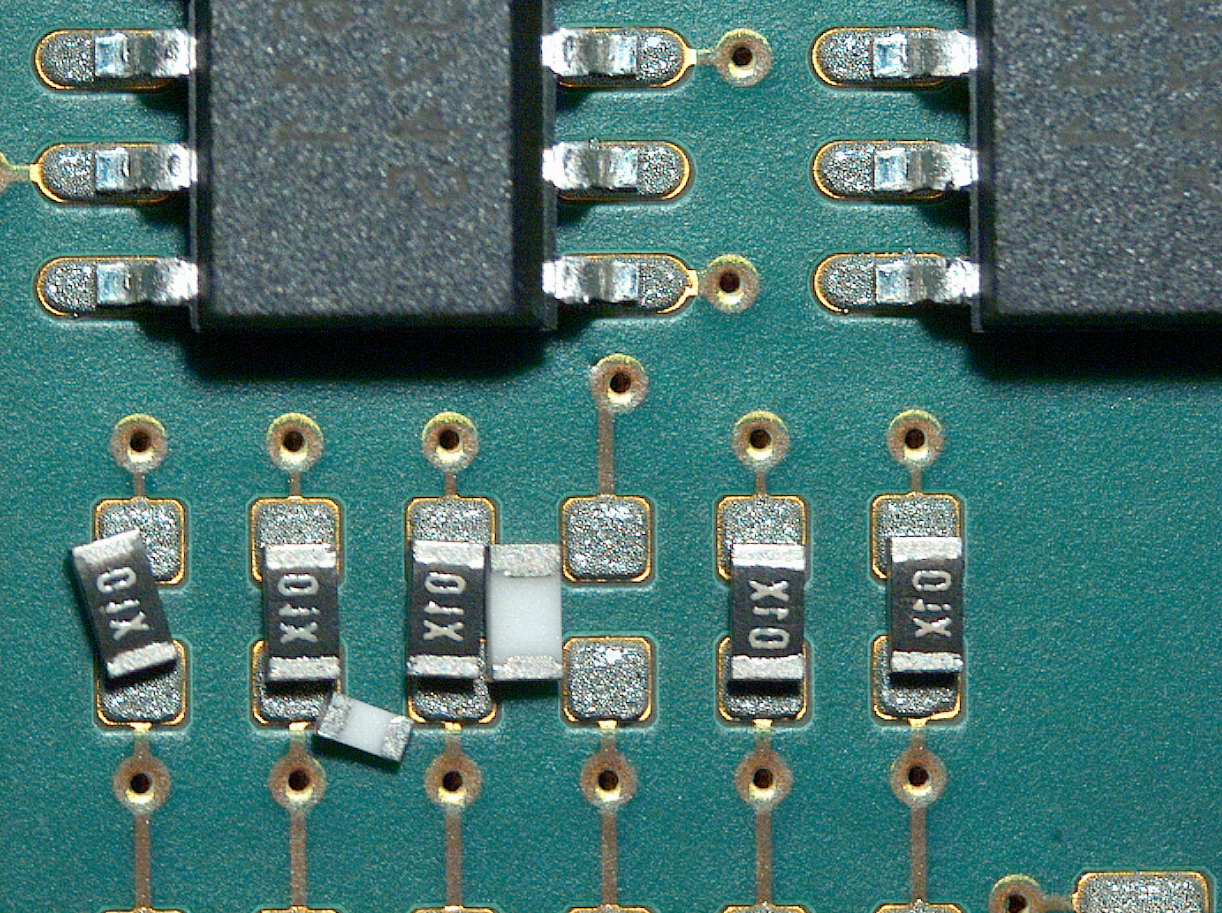
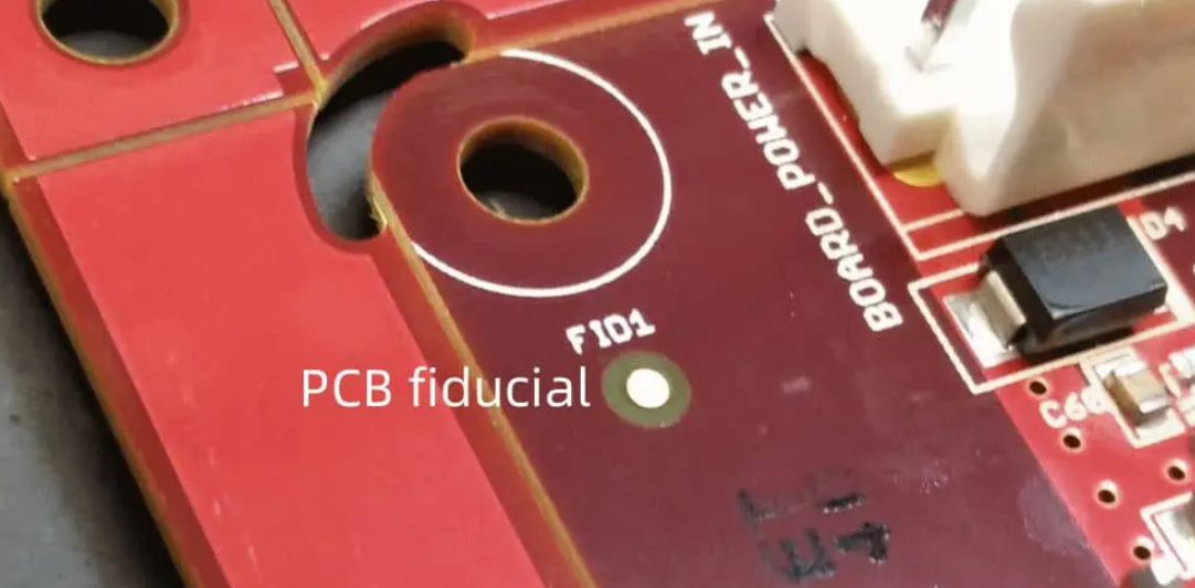
Several engineering factors govern component alignment on PCBs. First, PCB design includes fiducial marks, small copper pads used as reference points for positioning. These circular or cross-shaped features allow visual matching between the board and stencils or pickers. Warpage from manufacturing or handling distorts flatness, complicating alignment. Flat boards under 0.75% warpage, as per quality checks, provide the best base.
Component tolerances play a role too. Parts have specified body sizes and lead pitches that must fit land patterns designed accordingly. Surface tension during soldering pulls components toward pad centers if paste is applied evenly. However, uneven paste or contamination disrupts this self-alignment. Heat distribution affects movement, with reflow ovens providing controlled profiles unlike handheld irons.
Adherence to standards ensures consistency. J-STD-001J specifies requirements for soldered assemblies, including placement verification before and after reflow. These principles guide hobbyists in predicting behavior. Understanding them helps select appropriate methods for manual work. Thermal expansion differences between components and boards also influence final positioning.

Practical Best Practices for DIY PCB Component Alignment
DIY PCB component alignment starts with preparation. Clean the PCB surface thoroughly to remove oils or residues that cause slipping. Use isopropyl alcohol and lint-free wipes for this step. Inspect parts under magnification for bent leads or damage. Organize components by type to streamline workflow. A well-lit, static-free workspace minimizes errors from the outset.
Manual Component Placement Tips
Manual component placement tips revolve around steady hands and visual aids. Hold tweezers at a 45-degree angle to gently position SMD parts. Start with larger components to anchor the board, then fill in smaller ones. Use the "heel-toe" method for chips: align one end fully, then adjust the other to center. For through-hole parts, insert leads straight and trim excess before soldering. Practice on scrap boards builds muscle memory.
Avoid rushing; place one row at a time and verify before moving on. Rotate the board for better access to tight spots. If a part shifts, lift it with a toothpick rather than fingers to prevent contamination. These tips reduce misalignment from handling. Consistency yields repeatable results across projects.
Basic Alignment Tools for Hobbyists
Basic alignment tools make DIY work accessible without big investments. A digital microscope or loupe provides 10x to 50x magnification for spotting offsets. Alignment jigs, simple frames with pins matching board holes, hold PCBs flat and square. Vacuum pens pick up tiny parts without damage, releasing them precisely onto pads.
Stencil holders ensure repeatable paste application, indirectly aiding alignment. Laser pointers or alignment rulers help match fiducials across the board. These tools fit hobbyist budgets and spaces. Combine them for efficiency, like using a microscope with a jig. Over time, they pay off by cutting rework.
Solder Paste Alignment Techniques
Solder paste alignment techniques are crucial for reflow soldering in DIY setups. Apply paste via stencil, pressing firmly and scraping evenly for uniform deposits. Align the stencil using fiducials before spreading. Lift slowly at a 45-degree angle to avoid smearing. For manual paste, use syringes with fine tips, depositing beads centered on pads.
Preheat the board gently to improve paste tackiness, holding components in place. Verify alignment post-paste before reflow. Techniques like these prevent floating during melting. Adjust paste volume to match component size. Practice on test strips refines your approach.
Troubleshooting Common Alignment Issues
Troubleshooting alignment starts with identifying root causes. If components tombstone, check for uneven paste or rapid heating. Slow ramp-up in a reflow oven or hot plate resolves this. Skewed parts often result from airflow or board tilt; secure the assembly flat. Bridges form from excess paste or over-placement; clean with braid post-reflow.
Warped boards shift components; flatten under weights before assembly. Per IPC-A-610J criteria, verify leads cover at least 75% of pad length without specifics fabricated. Sticky flux helps reposition stubborn parts. Document issues per project for patterns. Systematic checks post-placement catch problems early.
For persistent offsets, revisit fiducial use or tool calibration. Through-hole misalignment stems from oversized holes; use fixtures. Reflow anomalies like drawbridging link to pad design, but manual tweaks suffice for hobbyists. Patience and iteration perfect skills.
Conclusion
Precision in PCB component alignment elevates DIY projects from prototypes to reliable builds. Key principles like fiducials and surface tension guide effective practices. Manual tips, basic tools, and solder paste techniques equip hobbyists for success. Troubleshooting common issues reinforces learning. Reference standards such as J-STD-001J for best outcomes. Apply these steps to create electronics that perform consistently.
FAQs
Q1: What are effective DIY PCB component alignment strategies for beginners?
A1: DIY PCB component alignment strategies include using fiducials for reference, magnification for verification, and paste tackiness for holding position. Start with larger parts, employ tweezers carefully, and check alignment before reflow. Secure the board flat to counter warpage. These steps minimize defects in home setups. Follow standards like IPC-A-610J for guidance on acceptability.
Q2: How can manual component placement tips improve my PCB assembly?
A2: Manual component placement tips focus on steady handling with tweezers, sequential placement from large to small, and the heel-toe alignment method. Use a lighted magnifier to spot offsets early. Avoid finger oils by wearing gloves. Practice on test boards builds accuracy. These practices reduce soldering rework significantly for hobbyists.
Q3: What basic alignment tools are essential for hobbyist PCB work?
A3: Basic alignment tools for hobbyists include digital microscopes for inspection, vacuum pens for picking tiny parts, and simple jigs for board fixturing. Stencil holders aid paste application. These affordable options replace automation. Combine with good lighting for best results. They ensure precise positioning without professional equipment.
Q4: Why are solder paste alignment techniques important in reflow soldering?
A4: Solder paste alignment techniques ensure even deposits matching pad footprints, enabling surface tension to center components during reflow. Use stencils aligned to fiducials and scrape uniformly. Preheat for better tack. Poor techniques cause shifts or bridges. Mastering them yields clean joints per J-STD-001J requirements.
References
IPC-A-610J — Acceptability of Electronic Assemblies. IPC, 2024
J-STD-001J — Requirements for Soldered Electrical and Electronic Assemblies. IPC, 2024


