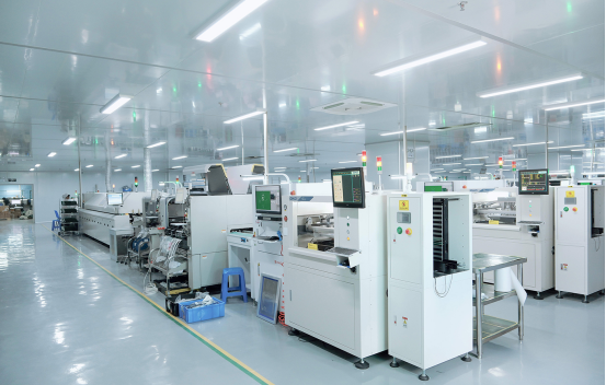
Introduction
High density PCB assembly demands precision at every step, where even minor deviations in component placement can lead to catastrophic failures. Component alignment testing verifies that parts sit correctly on their pads before and after reflow soldering, critical for boards packed with fine-pitch BGAs, QFNs, and 0201 passives. As miniaturization challenges push component density higher, misalignment risks electrical shorts, opens, and poor signal integrity. Electrical engineers face these issues routinely in designs for telecom, automotive, and medical devices. This article explores alignment testing methods, common pitfalls, and best practices to boost reliability. By mastering these techniques, teams can achieve yields above 99% in production runs.
Understanding Component Alignment in High-Density PCBs
Component density alignment refers to the precise positioning of parts relative to solder pads, measured in microns for high density PCB assembly. Tolerances tighten to 50 microns or less for pitches under 0.4mm, where offsets cause tombstoning or bridging during reflow. Fiducial marks serve as reference points, enabling pick-and-place machines to compensate for board warp or stencil shifts. Without proper alignment, thermal stresses exacerbate joint defects, reducing mean time between failures. Industry standards like IPC-A-610 outline acceptability criteria for placement offsets across classes 2 and 3 assemblies. Engineers must integrate these checks early to avoid costly rework.
In high-density designs, alignment matters because signal paths shrink, amplifying crosstalk from shifted components. Misplaced high-speed parts disrupt impedance control, violating design rules. Component density alignment also affects testability, as probes fail on offset pads. Proactive testing identifies issues pre-reflow, saving time over post-solder fixes. For electrical engineers, quantifying alignment via metrics like Cpk ensures process capability exceeds 1.33.
Key Challenges in Miniaturization and Alignment
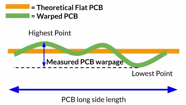
Miniaturization challenges dominate high density PCB assembly, starting with board warpage from CTE mismatches between copper, laminate, and silicon dies. A 0.5% warp over 100mm translates to 500 micron offsets, exceeding tolerances for 0.3mm pitch devices. Solder paste volume variations during printing compound this, as uneven deposits pull components during reflow. High component density limits fiducial placement, forcing reliance on edge or local marks prone to panelization errors. Dust or residue on fiducials further degrades machine vision accuracy.
Another hurdle involves feeder inaccuracies in pick-and-place, where vibration or nozzle wear causes theta rotation up to 2 degrees on tiny parts. Reflow ovens introduce ramp-soak-peak profiles that shift bottom-terminated components if paste is insufficient. Troubleshooting these requires isolating variables, like correlating placement logs with X-ray post-reflow images. Electrical engineers often overlook stencil wear, which smears paste and mimics alignment faults. Addressing these systematically prevents yield drops from 95% to below 80%.
Technical Principles of Component Alignment Testing
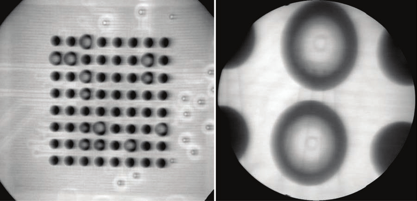
Alignment testing hinges on optical recognition of fiducials, typically 1mm diameter copper pads with cleared annuli for contrast. Machines calculate offsets in X, Y, and rotation (theta), adjusting nozzles in real-time per IPC-9850 guidelines for placement accuracy. Repeatability tests place 100 parts, measuring standard deviation below 20 microns for class 3 boards. Pre-reflow, solder paste inspection (SPI) uses 3D laser profiling to confirm deposit alignment with stencils. Post-placement, automated optical inspection (AOI) scans for offsets, bridging, or tombstoning.
For hidden joints like BGAs, X-ray laminography reveals ball offsets without slicing boards. Slice imaging reconstructs layers, quantifying grid array shifts to 10 microns. These methods scale with density, handling 10 million pads per panel. Engineers calibrate systems using golden boards with known fiducials, establishing baselines. J-STD-001 criteria guide solder fillet formation, tying back to initial placement quality.
Advanced Alignment Methods for High-Density Assemblies
Advanced alignment methods leverage machine learning in AOI for defect classification, reducing false calls by 30% on dense boards. Dual-camera systems with telecentric lenses eliminate parallax errors, achieving sub-10 micron resolution. Local fiducials near fine-pitch areas outperform globals, compensating for localized warp. Jet printing replaces stencils for volumes under 50 microns, minimizing volume-induced shifts.
Process optimization includes nitrogen reflow to stabilize paste flow, cutting shifts by 15%. Closed-loop feedback from SPI to placement adjusts feeders dynamically. For troubleshooting, engineers analyze Cpk data: below 1.0 signals feeder issues, while post-reflow theta errors point to ramp rates. Panel depanelization timing affects edges, so score-and-break post-bake preserves fiducials. These methods ensure component density alignment meets specs across volumes.
Best Practices and Troubleshooting in Practice
Start with design rules: place three globals per panel corner, locals every 50mm, avoiding vias or silkscreen overlap. Verify Gerber-to-Gerber alignment pre-fab using CAM software offsets. In assembly, run machine self-tests per IPC-9850, targeting 2Cpk minimum. Calibrate nozzles weekly, logging variances. For miniaturization challenges, thin boards under 0.8mm need vacuum fixturing to flatten during placement.
Troubleshooting misalignment begins with placement verification: if offsets exceed 25% pad size, check feeders first. SPI flags low-volume sites; add tacky flux for hold-down. Post-reflow X-ray tombstoning implicates paste asymmetry, resolved by stencil snap-off optimization. Warpage over 0.75% I/Os demands sequential lamination or low-CTE cores. Track first-pass yields, correlating to machine uptime. Electrical engineers benefit from Pareto charts, prioritizing top defects like rotation from nozzle skips.
A practical case involved a 0.35mm pitch FPGA board hitting 5% tombstoning. Root cause was 30 micron SPI offsets from stencil wear; switching to laser-cut stencils and local fiducials dropped it to 0.2%. X-ray confirmed BGA grid alignment post-fix. Such diagnostics underscore iterative testing.
Conclusion
Component alignment testing anchors reliability in high density PCB assembly, countering miniaturization challenges through precise fiducials, advanced inspection, and standards compliance. Electrical engineers armed with IPC guidelines and troubleshooting flows minimize defects, ensuring robust performance. Prioritize process controls for sustained high yields. Future trends like 0.2mm pitches demand even tighter methods, but fundamentals endure.
FAQs
Q1: What are the main causes of component misalignment in high density PCB assembly?
A1: Warpage from CTE mismatch, stencil misalignment, and feeder inaccuracies top the list. Insufficient solder paste volume causes reflow shifts, while poor fiducials degrade machine vision. Troubleshooting starts with SPI data review and nozzle calibration. Adhering to IPC-A-610 criteria prevents most issues, maintaining offsets under 50 microns.
Q2: How do advanced alignment methods address miniaturization challenges in PCBs?
A2: Methods like 3D SPI, AOI with ML, and X-ray laminography provide sub-10 micron precision for fine pitches. Local fiducials compensate warp, while closed-loop feedback auto-corrects placements. Nitrogen reflow stabilizes joints. These ensure component density alignment amid shrinking footprints, boosting yields for dense designs.
Q3: What role does IPC-9850 play in component density alignment testing?
A3: IPC-9850 standardizes pick-and-place accuracy metrics, including X, Y, theta repeatability via test matrices. It guides Cpk calculations for process capability. Engineers use it to benchmark machines, targeting under 20 micron sigma. This directly tackles high density PCB assembly variability.
Q4: Why is fiducial placement critical for high density PCB assembly?
A4: Fiducials enable precise board-to-machine registration, correcting warp up to 0.5%. Globals handle panels, locals fine-tune dense zones. Poor placement leads to offsets amplifying in reflow. Best practice: 1mm diameter with 0.1mm annuli clearance. This supports miniaturization challenges effectively.
References
IPC-A-610H — Acceptability of Electronic Assemblies. IPC, 2020
IPC J-STD-001H — Requirements for Soldered Electrical and Electronic Assemblies. IPC, 2018
IPC-9850A — Surface Mount Placement Equipment Characterization. IPC, 2011


