Introduction
Wave soldering remains the most efficient method for soldering through-hole components and mixed-technology boards in medium-to-high volume production. A properly set-up wave solder machine can achieve defect rates below 100 ppm while processing hundreds of boards per hour. This beginner-friendly guide covers machine basics, process parameters, proven soldering techniques, common defects with solutions, and daily maintenance practices used on real production lines.
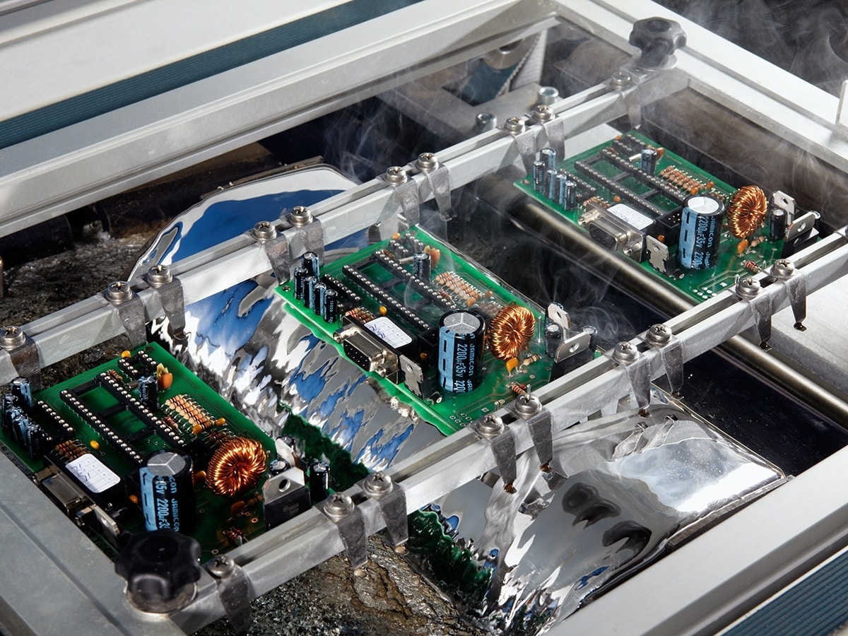
Wave Soldering Process Overview
- Flux application (spray or foam)
- Preheating (activates flux, reduces thermal shock)
- First wave (turbulent wave for wetting)
- Second wave (laminar wave for cosmetic fillet)
- Cooling (controlled or forced air)
Modern machines use inert nitrogen atmosphere to reduce dross and improve wetting on difficult finishes.
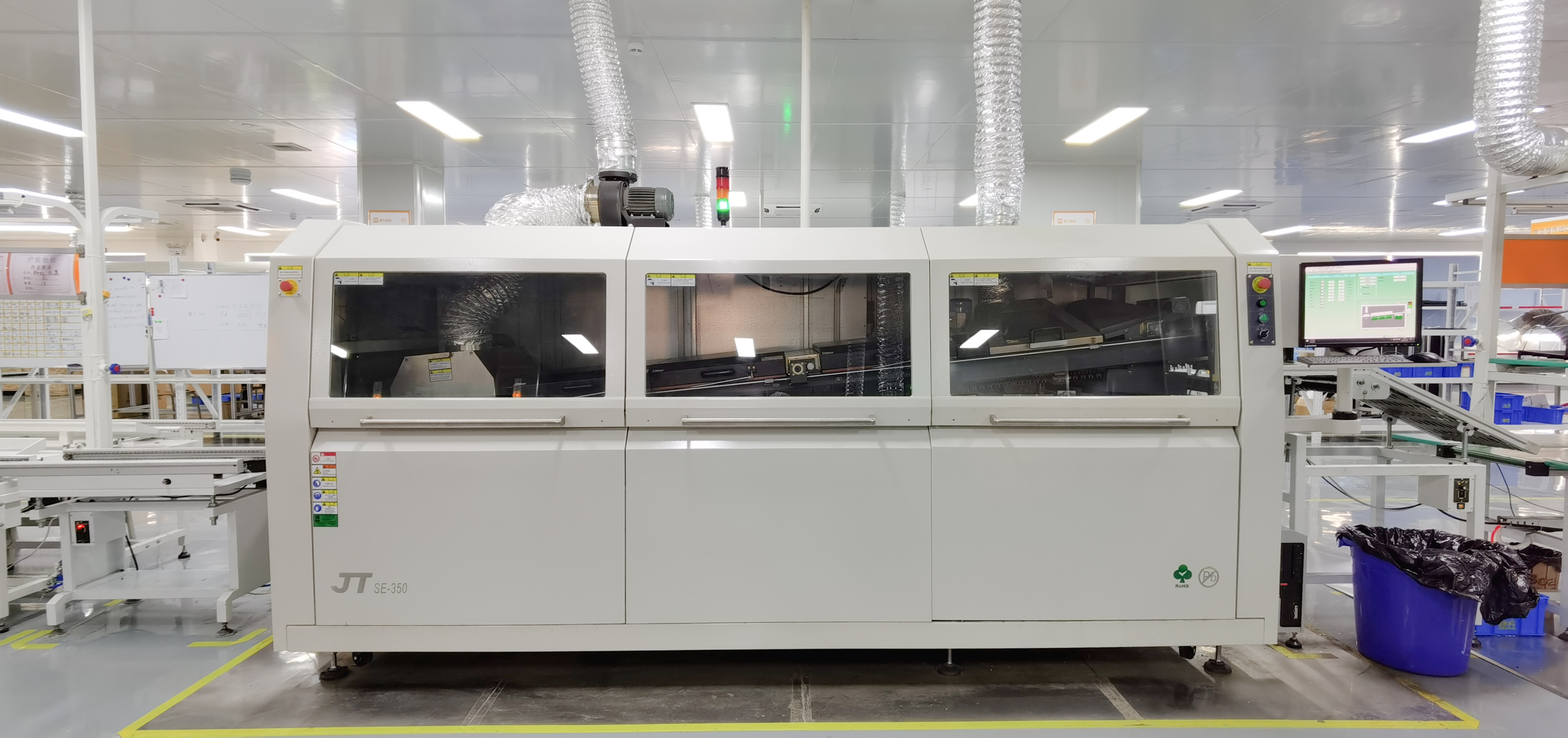
Essential Wave Solder Machine Components
- Spray fluxer with adjustable pressure and stroke
- Convection or IR preheat zones (top and bottom)
- Single or dual wave (chip wave + main wave)
- Titanium solder pot and pump system
- Conveyor with adjustable angle (4–7° typical)
Key Process Parameters and Beginner Settings
|
Parameter |
Recommended Starting Value |
Purpose |
|
Conveyor speed |
1.0–1.5 m/min |
Contact time control |
|
Preheat top/bottom |
90–110 °C board temperature |
Flux activation, thermal shock reduction |
|
Solder pot temperature |
255–265 °C (lead-free) |
Proper fluidity and wetting |
|
Wave height |
60–70 % of board thickness |
Full pin contact without bridging |
|
Conveyor angle |
6° |
Peel-off direction to reduce bridges |
|
Nitrogen flow |
800–1200 L/min |
Reduce dross and improve wetting |
Proven Soldering Techniques for Best Results
For fast turn PCB fabrication, wave solder reliability depends heavily on disciplined design and preparation.
- Pallet design: Use selective pallets for double-sided SMT boards
- Component orientation: Align long axes perpendicular to wave travel
- Pin protrusion: 1.0–2.0 mm above board bottom
- Thermal relief: Always use proper spoke patterns on planes
- Board cleanliness: Bake boards 4 h at 105 °C if stored > 3 months
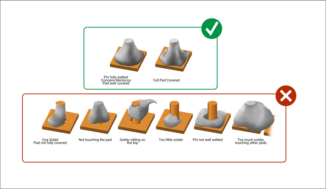
Common Soldering Defects and Fixes
|
Defect |
Typical Cause |
Solution |
|
Bridging |
Too slow speed, wrong peel-off, excess solder |
Increase conveyor speed, adjust angle to 6–7° |
|
Icicles/skewers |
Cold wave, poor flux activity |
Raise pot temperature 5–10 °C, check flux density |
|
Insufficient fill |
Short contact time, oxidized pins |
Lower wave height slightly, increase immersion |
|
Solder balls |
Excessive flux, moisture in board |
Reduce flux volume, pre-bake boards |
|
Dull/grainy joints |
Contaminated solder pot |
Regular dross removal, weekly pot cleaning |
Daily and Weekly Maintenance Tips
Daily
- Empty dross from wave nozzles
- Clean flux nozzles with IPA
- Check oil level in pump system
- Wipe titanium fingers and conveyor rails
Weekly
- Drain and filter solder pot (nitrogen machines)
- Calibrate temperature sensors
- Inspect pump impeller for wear
- Clean preheaters and exhaust filters
Lead-Free vs Leaded Wave Soldering
|
Parameter |
Sn63/Pb37 (Leaded) |
SAC305 (Lead-Free) |
|
Pot temperature |
245–255 °C |
260–270 °C |
|
Preheat target |
80–100 °C |
100–120 °C |
|
Typical defects |
Less bridging |
More icicles |
|
Dross formation |
Moderate |
High (nitrogen helps) |
Conclusion
Wave soldering delivers consistent, high-quality through-hole joints in PCBA assembly when process parameters stay within narrow windows. Start with the baseline settings above, adjust one parameter at a time while monitoring defect rates, and maintain rigorous daily cleaning. A well-maintained modern wave solder machine routinely achieves first-pass yields above 99.5 % on properly designed boards.
FAQs
Q1: Can I wave solder double-sided SMT boards?
A1: Yes, using selective pallets that cover top-side components while exposing only through-hole pins. Proper pallet design prevents component movement.
Q2: How often should I change the solder pot completely?
A2: Every 6–12 months for lead-free, longer for leaded. Copper accumulation above 1.0 % requires full replacement.
Q3: Why do I get bridges only on certain connectors?
A3: Pin spacing and orientation. Connectors with pins parallel to wave travel bridge easily. Rotate 90° or use selective pallet with dedicated channels.
Q4: Is nitrogen really necessary for wave soldering?
A4: Not mandatory for simple leaded boards, but essential for reliable lead-free results and OSP finish boards.
References
IPC J-STD-001H — Requirements for Soldered Electrical and Electronic Assemblies. IPC, 2020.
IPC-7530A — Guidelines for Temperature Profiling for Mass Soldering Processes (Wave and Reflow). IPC, 2017.
IPC-A-610H — Acceptability of Electronic Assemblies. IPC, 2020.
IPC-HDBK-001H — Handbook and Guide to Supplement J-STD-001. IPC, 2020.


