Introduction
Crystal oscillators provide the precise timing signals essential for microcontrollers, communication systems, and embedded devices in modern PCB designs. However, crystal oscillator startup failure remains a frequent challenge during prototyping and production, leading to system resets, erratic behavior, or complete non-functionality. These issues often stem from subtle mismatches in circuit parameters or PCB layout issues that prevent reliable oscillation. For electrical engineers, understanding crystal oscillator troubleshooting is crucial to ensure robust performance across temperature and voltage variations. This article explores the root causes, including negative resistance deficiencies, ESR mismatches, and load capacitance errors, while offering structured debugging tips. By following these guidelines, PCB designers can minimize crystal oscillator startup failure risks and achieve consistent operation.
What Is Crystal Oscillator Startup Failure and Why It Matters
Crystal oscillator startup failure occurs when the circuit fails to initiate and sustain stable oscillation after power-up, resulting in no clock output or prolonged delay before oscillation begins. In Pierce oscillators, the most common configuration, this manifests as the absence of a sinusoidal waveform across the crystal terminals, often detectable via oscilloscope probing. Such failures disrupt timing-critical functions like UART communication, ADC sampling, or real-time processing, potentially causing cascading system errors. Reliability suffers particularly in battery-powered or harsh-environment applications where marginal conditions exacerbate the problem. Addressing crystal oscillator troubleshooting early prevents costly respins and ensures compliance with performance expectations. Ultimately, mastering these concepts elevates PCB design quality for electrical engineers focused on high-reliability boards.
The prevalence of this issue underscores its importance in the design workflow. Poor startup leads to intermittent faults that evade initial bench tests but fail field trials. Engineers must prioritize factors like negative resistance adequacy and PCB layout issues to mitigate risks. Proactive measures align with industry practices for stable timing references.
Technical Principles Behind Crystal Oscillator Operation
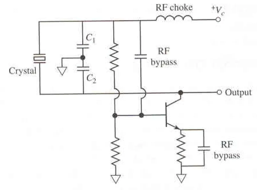
Crystal oscillators rely on the piezoelectric properties of quartz to resonate at a precise frequency, modeled as a series RLC circuit in parallel with shunt capacitance. In the Pierce topology, an inverter provides the necessary negative resistance to overcome the crystal's equivalent series resistance (ESR), enabling sustained oscillation. The active device's transconductance generates this negative resistance, which must exceed the ESR by a safety margin, typically ensuring reliable startup under varying conditions. Load capacitance, formed by external capacitors and PCB parasitics, tunes the resonance frequency and influences loop gain. Imbalances here directly contribute to crystal oscillator startup failure.
Negative resistance is pivotal: the circuit's feedback must produce a value whose magnitude is sufficiently larger than the ESR to compensate for losses and initiate oscillation from noise. Insufficient margin results in damping rather than amplification. ESR represents the mechanical damping in the crystal, higher in low-frequency units, demanding stronger drive capability. Load capacitance mismatches shift the operating point, reducing effective negative resistance or overdriving the crystal.
Power supply characteristics also play a role in startup dynamics. A slow voltage ramp fails to deliver the initial energy kick needed for oscillation buildup. Temperature affects ESR and capacitance stability, with extremes testing the design margins. PCB layout issues introduce stray inductances and capacitances that alter these parameters unexpectedly.
Common Causes of Crystal Oscillator Startup Failure
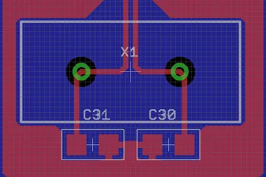
PCB layout issues top the list of culprits, as long traces add parasitic capacitance and inductance, detuning the load capacitance and weakening negative resistance. Vias in the oscillator loop introduce discontinuities, while ground plane splits create high-impedance return paths, amplifying noise susceptibility. Stray coupling from nearby high-speed signals injects interference, preventing clean startup. These factors compound in multi-layer boards where layer transitions exacerbate parasitics.
Component mismatches follow closely. Incorrect load capacitance, often due to unaccounted strays, reduces loop gain; the effective capacitance seen by the crystal deviates from datasheet specifications. High ESR crystals paired with marginal drive circuits fail to oscillate, especially at elevated temperatures where ESR rises. Feedback resistor values, if too high, starve the loop gain, while absent series damping resistors risk overdrive but aid startup.
Environmental and process factors contribute too. Slow power-on ramps delay energy buildup, particularly for low-frequency crystals. Contaminants like flux residues lower surface insulation resistance, shunting the circuit. Manufacturing variations in capacitor tolerances shift load capacitance, turning marginal designs into failures.
Adhering to IPC-2221 guidelines for trace routing and spacing helps mitigate many layout-induced issues.
Practical Solutions and Best Practices for PCB Designers
Start with precise load capacitance calculation: CL = (C1 * C2) / (C1 + C2) + Cstray, where Cstray includes PCB traces, pins, and sockets, typically estimated at 2-5 pF. Use high-stability NP0/COG capacitors matched to the crystal datasheet. Verify by measuring frequency shift or using network analysis on bare PCB.
For PCB layout, position the crystal within millimeters of the driving IC pins, using traces under 5 mm long and 0.15 mm wide. Avoid vias entirely in the loop; route symmetrically with a ground pour encircling the components, stitched with multiple vias for low impedance. Implement a guard ring or fenced ground trace around the oscillator to shield from crosstalk. Keep the area free of other signals, heat sources, or edges.
To ensure negative resistance adequacy, incorporate a test series resistor or potentiometer during prototyping. Increment until oscillation ceases; success with added resistance exceeding expected ESR confirms margin. Scope the crystal pins for startup waveform: expect noise buildup to sine within milliseconds. Test across voltage and temperature extremes, as high temperature and low voltage minimize gain.
Power supply design matters: use sharp rise times via decoupling capacitors close to the IC, low-ESR types. Add a series damping resistor if overdrive is suspected, balancing startup speed.
Following J-STD-001 requirements for soldering cleanliness prevents residue-related shunts.
Troubleshooting Crystal Oscillator Startup Failure Step-by-Step
Begin with visual inspection: confirm connections, capacitor values, and crystal orientation. Power up and probe with a low-capacitance scope: no signal indicates total failure, while weak or distorted waveforms suggest marginal gain. Check DC bias at gates for proper inverter operation.
Quantify loop gain: insert a variable resistor in series with the crystal. If oscillation holds beyond 2-3 times the datasheet maximum ESR, margin is adequate. Adjust load capacitors iteratively, monitoring frequency stability.
Isolate layout issues: review for ground loops or noise; relocate if coupling is evident. Measure parasitics with a vector network analyzer on an unpopulated board to refine CL calculation.
Environmental screening: bake boards to remove moisture and test at temperature chamber extremes. If intermittent behavior persists, suspect noise; add shielding.
Advanced: compute negative resistance from device transconductance and capacitances per formulas, simulating if tools are available.
Systematic application resolves most crystal oscillator troubleshooting cases efficiently.
Conclusion
Crystal oscillator startup failure demands attention to negative resistance, ESR, load capacitance, and PCB layout issues from the outset. By prioritizing short traces, precise calculations, and margin testing, designers avert common pitfalls. Rigorous verification across conditions ensures reliability. Integrating these practices streamlines development, reducing iterations. Electrical engineers equipped with these debugging tips deliver timing-stable PCBs ready for production.
FAQs
Q1: What causes crystal oscillator startup failure most often in PCB designs?
A1: PCB layout issues like long traces and poor grounding introduce parasitics that mismatch load capacitance and reduce negative resistance below ESR levels. Stray capacitance detunes the circuit, while noise coupling disrupts initiation. Testing with a series resistor confirms gain margin. Proper layout per design standards resolves most cases without component changes.
Q2: How do you troubleshoot negative resistance in crystal oscillators?
A2: Measure by adding a potentiometer in series with the crystal and increase it until oscillation stops, ensuring the added resistance exceeds ESR by 3-5 times. Scope waveforms for the noise-to-sine transition. Adjust feedback or damping resistors if marginal and account for temperature effects on transconductance. This approach quantifies startup reliability effectively.
Q3: What PCB layout best practices prevent crystal oscillator troubleshooting needs?
A3: Place the crystal near IC pins with traces under 5 mm, no vias, and an encircling ground pour. Symmetric routing minimizes imbalance. Isolate from high-speed lines with guard traces. Calculate load capacitance including strays. These steps maintain negative resistance superiority over ESR.
Q4: How does load capacitance affect crystal oscillator startup failure?
A4: Excessive load capacitance lowers loop gain, weakening negative resistance against ESR. Too low risks overdrive but can aid startup. Match the series equivalent to the datasheet CL plus parasitics. Verify with frequency measurement post-assembly. Trimmer capacitors aid fine-tuning during prototyping.
References
IPC-2221B — Generic Standard on Printed Board Design. IPC, 2012
IPC-6012E — Qualification and Performance Specification for Rigid Printed Boards. IPC, 2017
J-STD-001G — Requirements for Soldered Electrical and Electronic Assemblies. IPC, 2017
IPC-A-610H — Acceptability of Electronic Assemblies. IPC, 2019


