Introduction
Designing printed circuit boards for IPC Class 2 assembly requires careful attention to ensure reliable performance in dedicated service electronic products. Electrical engineers often face challenges in balancing functionality, manufacturability, and cost when targeting this classification. IPC Class 2 products demand higher reliability than general consumer goods but allow for some downtime with repair, making design choices critical for smooth assembly processes. This guide explores PCB design for IPC Class 2, focusing on component placement guidelines IPC Class 2, trace width and spacing for IPC Class 2 assembly, and design producibility levels IPC. By following these principles, engineers can minimize defects, reduce rework, and achieve consistent yields during surface mount technology operations.

What Is IPC Class 2 PCB Assembly and Why Does It Matter?
IPC Class 2 defines acceptability criteria for electronic assemblies intended for dedicated service, such as communication equipment, measurement devices, and computing hardware where performance on demand is essential. Unlike Class 1 for general electronics, Class 2 imposes stricter solder joint quality, cleanliness, and marking requirements to support longer operational life with occasional maintenance. For electrical engineers, adhering to these standards prevents field failures and ensures compatibility with standard assembly flows. Design decisions early in the process directly impact assembly success, as poor layout can lead to bridging, insufficient solder volume, or inspection rejects. Understanding IPC Class 2 matters because it aligns product reliability with cost-effective manufacturing, avoiding the over-design typical of Class 3 high-reliability applications.
Fundamental Design Principles for IPC Class 2 Assembly
Effective PCB design for IPC Class 2 starts with material selection and layer stackup that support thermal stability during reflow soldering. Engineers must consider board thickness, copper weight, and finish types to facilitate uniform heating and prevent warpage. Fiducial marks play a vital role in aligning pick-and-place machines accurately, reducing offset errors that could violate placement tolerances. Routing strategies should prioritize signal integrity while accommodating manufacturing variances inherent to Class 2 processes. These principles form the foundation for downstream assembly steps, including stencil printing and automated optical inspection.
Producibility levels outlined in industry standards guide feature complexity, with moderate levels suiting most Class 2 designs. Engineers evaluate trade-offs between density and ease of assembly, ensuring vias, pads, and traces align with equipment capabilities. Thermal management features, like copper pours, help dissipate heat from components without compromising solderability.
Component Placement Guidelines IPC Class 2
Component placement guidelines IPC Class 2 emphasize spacing that allows for accurate machine handling and visual inspection post-reflow. Engineers should group components by technology type, separating surface mount devices from through-hole parts to streamline soldering phases. Minimum distances between parts prevent shadowing during stencil printing, where solder paste might fail to release properly under adjacent shadows. Polarized components require clear orientation markers to avoid assembly errors, and tall profiles demand consideration of conveyor clearance in wave soldering setups.
In high-density areas, staggering rows reduces bridging risks during reflow, as molten solder flows more predictably with airflow gaps. Fiducials positioned at board corners and panel edges enable sub-50 micron placement accuracy, critical for fine-pitch devices common in Class 2 boards. Engineers troubleshoot placement by simulating reflow profiles, identifying potential tombstoning in components with mismatched thermal masses. Adhering to land pattern standards ensures toe and heel fillet formation meets acceptability criteria, minimizing open joints.
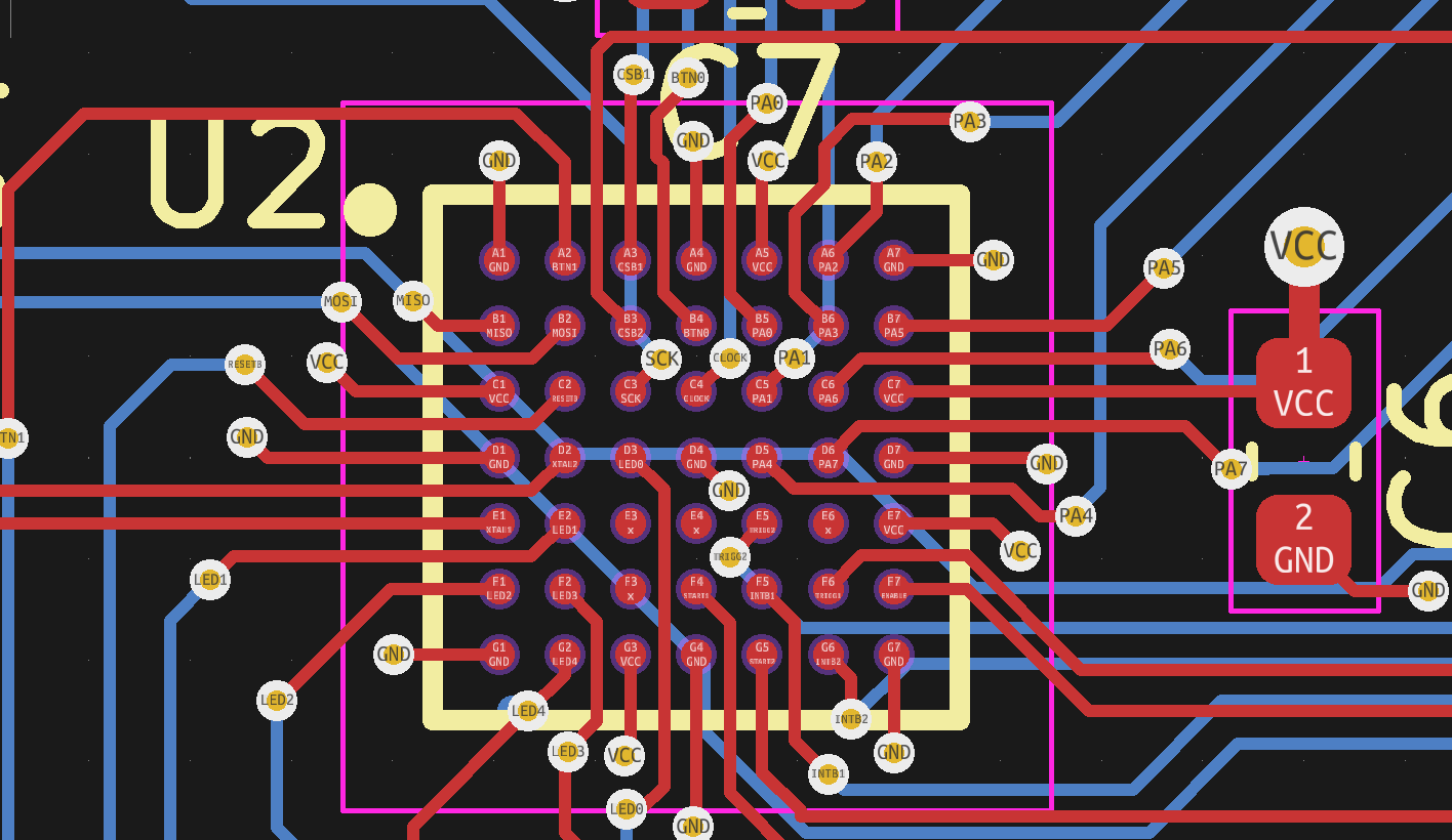
Placement near board edges requires reinforced keep-out zones to prevent peel-up during depaneling, a frequent cause of microcracks. Decoupling capacitors positioned close to power pins reduce noise, but spacing must allow probe access for in-circuit testing. These guidelines enhance first-pass yields, as tight placements often lead to rework cycles that inflate costs.
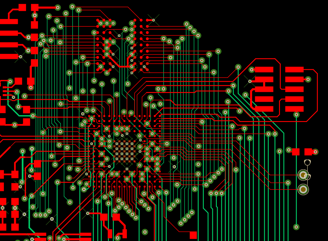
Trace Width and Spacing for IPC Class 2 Assembly
Trace width and spacing for IPC Class 2 assembly must account for current carrying capacity, voltage isolation, and etching tolerances. Wider traces handle higher currents with lower resistance, but excessive width crowds placement areas, complicating routing. Spacing prevents arcing in high-voltage sections and shorts from solder mask registration errors, common in multilayer boards. Engineers select spacings based on voltage differentials, ensuring creepage and clearance paths remain intact post-assembly.
Routing on inner layers benefits from ground planes that shield signals, but vias transitioning layers need annular rings sized for drill wander. Acute angles in traces promote acid trapping during etching, leading to undercuts that fail continuity tests. Curved or 45-degree bends improve manufacturability, distributing stress evenly during thermal cycling. Troubleshooting involves reviewing Gerber files for neck-downs, where traces narrow unintentionally due to design rule check oversights.
For mixed-signal boards, dedicated analog and digital zones with guard traces maintain integrity, spaced to block crosstalk. These practices align with generic design standards, supporting reliable impedance control without excessive prototyping.
Design Producibility Levels IPC
Design producibility levels IPC categorize features from most reliable to complex, helping engineers match board density to Class 2 capabilities. Level A offers maximum margins for drill sizes, trace etches, and pad overlaps, ideal for high-volume runs with standard tooling. Level B provides balanced density for typical dedicated service products, while Level C pushes limits for innovative layouts at higher risk. Selecting the appropriate level early prevents costly respins, as Level C features demand advanced equipment not always available for Class 2.
Producibility influences hole-to-pad ratios, where generous registration eases plating uniformity. Engineers assess overall board complexity, factoring in layer count and via density against fab capabilities. Troubleshooting low yields often traces back to mismatched levels, such as fine-line traces on budget panels prone to breakage.
Best Practices for IPC Class 2 PCB Assembly Success
Implement design for assembly by incorporating test points spaced for bed-of-nails fixtures, avoiding solder mask coverage issues. Solder mask expansion around pads prevents bridging, and silkscreen legends require clear fonts for automated verification. Panelization with breakaway tabs facilitates handling, positioned away from critical circuits to avoid stress cracks.
Thermal reliefs on thermal pads improve wetting without excessive heat sinking, crucial for QFN and BGA devices. Simulate solder paste volume using stencil thickness guidelines, adjusting aperture reductions for small components. Regular design reviews catch violations, ensuring compliance across teams.
Troubleshooting Common Issues in IPC Class 2 Designs
Warpage from asymmetric copper distribution causes component lifts during reflow, resolved by balancing pours across layers. Bridging in fine-pitch areas stems from excessive paste volume, fixed by finer stencil apertures or reduced print pressure. Insufficient barrel fill in vias indicates plating shortfalls, prompting larger aspect ratios.
Placement offsets arise from fiducial misalignment, corrected by global and local marks. Solder beading under components signals paste smearing, mitigated by zoned stencils. These fixes stem from iterative DFM analysis, boosting reliability.
Conclusion
Mastering design considerations for IPC Class 2 PCB assembly empowers electrical engineers to deliver robust, manufacturable boards. Key elements like component placement guidelines IPC Class 2, trace width and spacing for IPC Class 2 assembly, and design producibility levels IPC ensure alignment with industry expectations. Practical troubleshooting and best practices minimize risks, supporting efficient production. Prioritizing these factors yields high-reliability products at optimal costs, ready for demanding service environments.
FAQs
Q1: What are the main differences in PCB design for IPC Class 2 versus Class 3?
A1: IPC Class 2 allows moderate tolerances for solder joints and cleanliness, suiting dedicated service products, while Class 3 demands tighter criteria for high-reliability apps. Component placement guidelines IPC Class 2 permit larger offsets than Class 3, easing assembly but requiring vigilant inspection. Engineers select Class 2 for cost savings without sacrificing essential performance.
Q2: How do trace width and spacing for IPC Class 2 assembly impact yield?
A2: Adequate spacing prevents shorts from mask misalignment, directly boosting first-pass yields in reflow. Wider traces reduce resistance heating, aiding thermal balance. Troubleshooting narrow spacings reveals etching defects, prompting rule adjustments for consistent IPC Class 2 compliance.
Q3: What role do design producibility levels IPC play in Class 2 projects?
A3: Levels guide feature density, with B suiting most Class 2 boards for balanced manufacturability. Level A maximizes ease, ideal for high volumes. Engineers use them to avoid over-complexity, ensuring smooth transitions to assembly.
Q4: Why focus on fiducials in component placement guidelines IPC Class 2?
A4: Fiducials enable precise machine alignment, minimizing offsets in fine-pitch placement. Poor positioning causes systematic errors, leading to rejects. Proper implementation supports automated processes, critical for Class 2 efficiency.
References
IPC-A-610J — Acceptability of Electronic Assemblies. IPC, 2024
IPC-2221B — Generic Standard on Printed Board Design. IPC, 2003
IPC-7351C — Generic Requirements for Surface Mount Design and Land Pattern Standard. IPC, 2010
J-STD-001H — Requirements for Soldered Electrical and Electronic Assemblies. IPC, 2018


