Introduction
In the fast-paced world of electronics development, bringing a new product from concept to market requires meticulous planning and execution. For prototype printed circuit board (PCB) assembly, success hinges not just on functionality, but on the ease, efficiency, and reliability of the entire development process. As an assembly engineer, I advocate for a holistic strategy known as Design for Excellence (DFX). DFX in prototype assembly is not a single rule, but a comprehensive set of design guidelines that integrate considerations for manufacturing, assembly, and testing from the very outset. This integrated approach is crucial for avoiding costly mistakes, accelerating development, and ensuring a smooth transition from prototype to high-volume production.
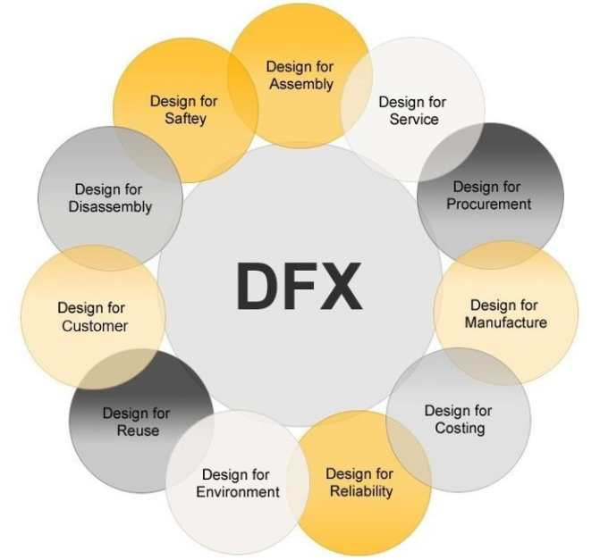
What is Design for Excellence (DFX) and its Holistic Importance for Prototypes
Design for Excellence (DFX) is an overarching philosophy that encompasses a multitude of design methodologies, each aimed at optimizing a specific aspect of a product's lifecycle. It is a broad term that includes practices like Design for Manufacturing (DFM), Design for Assembly (DFA), Design for Testability (DFT), Design for Reliability (DFR), and others. For prototype PCB assembly, applying DFX means proactively designing a board that is not only electrically sound but also inherently easy to build, test, and ultimately, manufacture at scale.
The holistic importance of DFX for prototypes cannot be overstated. Prototypes serve as the first tangible representation of a design, and they are critical for validating functionality, form, and fit. However, if a prototype is difficult to assemble, challenging to test, or costly to manufacture, it undermines the entire development effort. Issues discovered during prototype assembly can lead to:
- Significant design iterations and delays.
- Increased material and labor costs due to rework or scrap.
- Compromised reliability of the final product.
- Difficulty in scaling up to mass production.
By adopting a DFX approach, engineers move beyond isolated design goals. They consider the entire product lifecycle, ensuring that choices made during the schematic and layout phases positively impact every subsequent stage. This prevents downstream problems, making the prototype phase a true stepping stone to successful product launch, rather than a series of unexpected hurdles.
Core Pillars of DFX: Design for Manufacturing (DFM)
One of the foundational pillars of Design for Excellence (DFX) is Design for Manufacturing (DFM). For prototype assembly, DFM guidelines focus on ensuring that the PCB itself can be fabricated efficiently, accurately, and without defects. This involves optimizing the physical design of the board to match the capabilities of the chosen manufacturing process.
Key aspects of DFM for prototype PCB assembly include:
- Trace Widths and Spacing: Ensuring that the copper traces and spacing between them meet the fabricator's minimum capabilities. Insufficient spacing can lead to shorts, while overly thin traces may break or fail to carry required current. IPC-2221B, "Generic Standard on Printed Board Design," provides guidelines for trace geometries.
- Annular Ring Requirements: Verifying that the copper pad surrounding a drilled hole has adequate width. Insufficient annular rings can lead to "breakout" during drilling, compromising electrical connection and mechanical strength.
- Drill Hole Sizes and Tolerances: Specifying drill diameters and their tolerances within the manufacturer's standard capabilities to avoid increased costs or fabrication issues.
- Copper Weight: Matching the specified copper weight to the application's electrical requirements and the manufacturer's standard processes.
- Panelization Strategy: For designs that might eventually be panelized for efficiency, considering basic panelization guidelines even at the prototype stage can save time later. This includes proper spacing between individual boards and defining break-away features.
- Material Selection: Choosing PCB laminate materials that are standard and readily available, while meeting electrical and thermal requirements, helps reduce lead times and costs for prototypes.
By adhering to DFM guidelines, designers can prevent fabrication defects, ensure the integrity of the bare board, and lay a solid groundwork for the subsequent assembly process.
Related Reading: Design for Manufacturability (DFM): The Key to Reducing PCB Component Assembly Costs
Core Pillars of DFX: Design for Assembly (DFA)
Complementing DFM, Design for Assembly (DFA) is another critical component of the holistic design for excellence (DFX) strategy, especially for prototype PCB assembly. DFA focuses on optimizing the PCB layout and component selection to facilitate efficient, repeatable, and error-free component placement and soldering.
Effective DFA guidelines for prototype PCB assembly include:
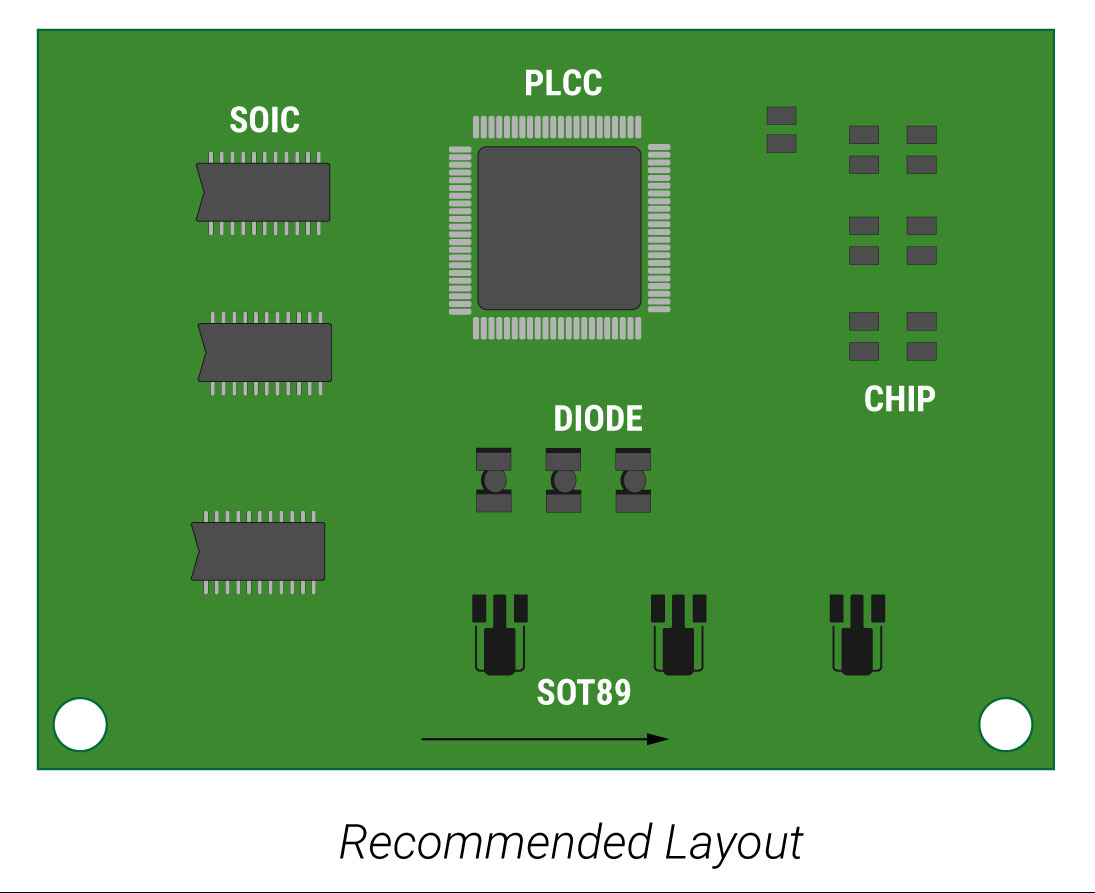
- Component Selection: Prioritizing standard, readily available components that are compatible with automated pick-and-place machinery. Using unusual or odd-form components can necessitate manual placement, increasing assembly time and cost.
- Component Spacing and Clearance: Ensuring sufficient space between components to allow for pick-and-place nozzle access, visual inspection, and rework. Too little space can lead to tombstoning, bridging, or difficulty in repair.
- Consistent Component Orientation: Orienting similar polarized components (e.g., diodes, electrolytic capacitors, ICs with pin 1) in the same direction whenever possible. This minimizes machine setup changes and reduces the risk of incorrect orientation errors during automated assembly.
- Fiducial Marks: Including global and local fiducial marks on the PCB layout. These optically recognizable targets provide reference points for automated assembly equipment, ensuring precise component placement. IPC-7351B, "Generic Requirements for Surface Mount Design and Land Pattern Standard," details fiducial requirements.
- Pad Geometry Optimization: Designing solder pads (land patterns) that are robust for soldering. Incorrect pad sizes or shapes can lead to poor solder joint formation, such as insufficient fillets or solder bridging. J-STD-001G, "Requirements for Soldered Electrical and Electronic Assemblies," provides criteria for acceptable solder joints.
- Test Point Accessibility: While primarily a DFT concern, accessible test points also simplify troubleshooting during prototype assembly, as they allow for easier probing and verification of connections.
By incorporating DFA guidelines, designers make the assembly process itself smoother and more reliable, reducing the chances of manufacturing-induced defects and the need for costly manual rework in prototype batches.
Related Reading: Design for Assembly (DFA) Considerations for High Density PCBs
Core Pillars of DFX: Design for Testability (DFT)
The third crucial pillar of Design for Excellence (DFX) in prototype assembly is Design for Testability (DFT). DFT guidelines ensure that the PCB can be efficiently and thoroughly tested to verify its functionality and identify any manufacturing or design flaws. Without adequate testability, even a perfectly manufactured board might be difficult to debug, leading to significant delays.
Key DFT guidelines for prototype PCB assembly include:
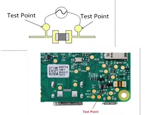
- Test Point Allocation: Incorporating sufficient test points or pads on the PCB layout to allow access for in-circuit testing (ICT) or functional testing (FCT) probes. These test points provide crucial access for electrical measurements.
- Test Point Placement: Strategically placing test points to maximize test coverage. This means providing access to critical nodes, component inputs/outputs, power rails, and ground connections.
- Net Access: Ensuring that every net (unique electrical connection) on the PCB has at least one accessible test point. This allows for comprehensive shorts and opens testing.
- Boundary Scan (JTAG): For complex digital circuits, implementing boundary scan architecture (IEEE 1149.1 standard) allows for testing interconnects and components without direct physical access to every pin, greatly simplifying test development.
- Power and Ground Access: Providing dedicated test points for power supply rails and ground to facilitate voltage measurements and power integrity checks.
- In-Circuit Test (ICT) Compatibility: Designing the board to be compatible with ICT fixtures, which require a "bed-of-nails" approach. This includes sufficient clearance around components for probe placement.
- Self-Test Capabilities: For more advanced prototypes, incorporating basic self-test routines into embedded firmware can provide initial functional verification without external test equipment.
By focusing on DFT, engineers ensure that faults can be quickly and accurately diagnosed, accelerating the debugging process for prototypes and guaranteeing that functional boards proceed to the next stage of development with confidence.
Integrating DFX Guidelines for a Comprehensive Prototype Strategy
The true power of Design for Excellence (DFX) in prototype assembly emerges when DFM, DFA, and DFT guidelines are integrated holistically rather than being treated as separate, independent considerations. This comprehensive prototype strategy ensures that every design decision serves multiple purposes, leading to an optimized product development cycle.
For instance, consider the placement of a large integrated circuit. A DFM perspective would ensure its pad geometry is correct for fabrication. A DFA perspective would dictate consistent orientation and sufficient clearance for automated placement and soldering. A DFT perspective would demand accessible test points on its key pins for electrical verification. An integrated DFX approach considers all these factors simultaneously, leading to a placement that is not only electrically sound but also easy to manufacture, assemble, and test.
This integration fosters a synergistic relationship between design, fabrication, and assembly teams. Design engineers, armed with DFX knowledge, can anticipate potential manufacturing challenges and proactively incorporate solutions into their layouts. Manufacturing specialists can provide early feedback on feasibility and cost implications. Assembly engineers, like myself, can offer insights into component handling, soldering processes, and rework strategies.
By continuously applying and refining DFX guidelines throughout the prototype development lifecycle, teams can:
- Minimize design iterations, saving time and resources.
- Improve the first-pass yield of assembled prototypes.
- Enhance the reliability and quality of the final product.
- Accelerate the transition from prototype to full-scale production, as the design is already optimized for manufacturing.
This holistic approach is not just about avoiding mistakes; it is about building a foundation for consistent excellence in all stages of product realization. Adherence to overarching quality standards, such as those found in ISO 9001:2015, "Quality Management Systems," further reinforces the commitment to a comprehensive DFX strategy.
Conclusion
The pursuit of excellence in prototype PCB assembly necessitates a holistic approach embodied by Design for Excellence (DFX). By meticulously integrating Design for Manufacturing (DFM) to optimize board fabrication, Design for Assembly (DFA) to streamline component placement and soldering, and Design for Testability (DFT) to ensure efficient verification, engineers can preempt a wide array of costly mistakes. This comprehensive DFX strategy is not just about isolated improvements; it creates a synergistic environment where every design decision contributes to enhanced manufacturability, faster assembly, reliable testing, and ultimately, a smoother transition from prototype to high-volume production. Embracing DFX guidelines from the outset is the most effective way to ensure the success and quality of electronic products.
FAQs
Q1: What does Design for Excellence (DFX) mean for prototype PCB assembly?
A1: Design for Excellence (DFX) for prototype PCB assembly is a comprehensive approach that integrates various design methodologies, such as Design for Manufacturing (DFM), Design for Assembly (DFA), and Design for Testability (DFT). Its goal is to optimize the prototype design to be inherently easy to fabricate, assemble, and test, thereby avoiding costly mistakes and delays.
Q2: How do Design for Assembly (DFA) guidelines impact prototype assembly?
A2: Design for Assembly (DFA) guidelines are crucial for prototype assembly as they focus on optimizing component placement and selection to streamline the assembly process. This includes ensuring adequate spacing, consistent component orientation, and proper pad designs, all of which reduce assembly errors, minimize rework, and improve overall assembly efficiency in prototype batches.
Q3: Why is Design for Testability (DFT) essential during prototype development?
A3: Design for Testability (DFT) is essential during prototype development to ensure the board can be thoroughly and efficiently tested. By incorporating features like accessible test points and considering boundary scan, DFT guidelines enable quick fault diagnosis, accelerate debugging, and confirm functional integrity, which is vital for validating prototypes.
Q4: What is the relationship between Design for Manufacturing (DFM) and Design for Excellence (DFX)?
A4: Design for Manufacturing (DFM) is a core component within the broader framework of Design for Excellence (DFX). DFM guidelines specifically focus on optimizing the PCB design for efficient fabrication, ensuring that the bare board can be produced without defects. DFX takes a holistic view, integrating DFM with other considerations like DFA and DFT to optimize the entire product lifecycle from prototype onwards.
References
IPC-A-610G — Acceptability of Electronic Assemblies. IPC, 2017.
IPC-2221B — Generic Standard on Printed Board Design. IPC, 2012.
IPC-7351B — Generic Requirements for Surface Mount Design and Land Pattern Standard. IPC, 2010.
J-STD-001G — Requirements for Soldered Electrical and Electronic Assemblies. IPC/JEDEC, 2017.
ISO 9001:2015 — Quality Management Systems. ISO, 2015.


