Introduction
Through-hole assembly remains a cornerstone in PCB design for applications demanding mechanical robustness and high current handling. Proper design rules ensure reliable solder joints, ease of insertion, and long-term durability under thermal and mechanical stress. Optimizing through-hole component placement, through-hole pad size, through-hole hole size, through-hole component spacing, and overall design for manufacturability through-hole directly impacts yield rates and field performance. Electrical engineers must balance density with producibility to avoid common pitfalls like lead damage or insufficient solder fill. This article explores structured guidelines drawn from established industry practices to enhance PCB layout efficiency. By adhering to these principles, designs achieve higher reliability without compromising on space constraints.
Understanding Through-Hole Assembly and Its Importance
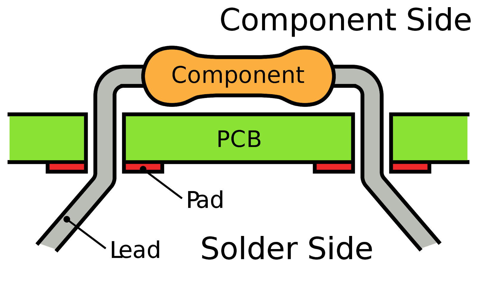
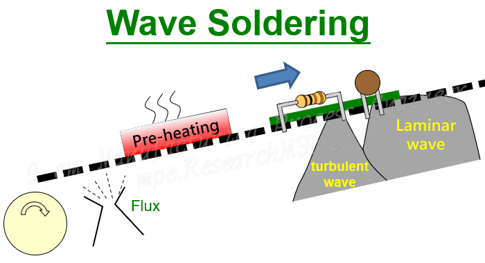
Through-hole technology involves inserting component leads through drilled holes in the PCB, followed by soldering on the opposite side, typically via wave or selective soldering. This method excels in scenarios requiring strong mechanical bonds, such as power electronics, connectors, and electromechanical devices, where surface-mount alone may falter. Unlike SMT, through-hole provides superior standoff for heat dissipation and vibration resistance, making it vital for automotive, aerospace, and industrial controls. However, poor layout can lead to assembly defects, increased costs, and reliability failures like cracked barrels or cold joints. Design for manufacturability through-hole emphasizes clearances, tolerances, and flow dynamics to streamline production. Engineers prioritizing these rules minimize rework and support mixed-technology boards effectively.
The relevance intensifies in high-reliability sectors, where IPC standards dictate minimum criteria for joint integrity. Through-hole component placement influences solder wave exposure uniformity, while precise through-hole pad size and hole size prevent plating voids or breakout. Inadequate through-hole component spacing risks bridging during soldering, compromising electrical isolation. Ultimately, these rules bridge design intent with fabrication capabilities, ensuring boards meet performance specs across lifecycles.
Key Technical Principles for Through-Hole Design
Central to through-hole design are the relationships between hole size, pad dimensions, and annular ring, governed by producibility levels in standards like IPC-7251. The finished hole diameter must accommodate the maximum lead diameter plus a clearance factor to allow easy insertion and plating uniformity. For density level A, suited to robust applications, this clearance is typically the maximum lead diameter plus 0.25 mm; level B uses 0.20 mm, and level C employs 0.15 mm for high-density boards. These factors account for lead tolerances, drill wander, and plating buildup, preventing tight fits that damage components or hinder solder wicking. Engineers select the level based on assembly process and risk tolerance, with level B serving most general purposes.
Through-hole pad size derives from the hole diameter plus twice the annular ring excess plus fabrication tolerances, as outlined in IPC-2221A. Annular ring excess values are 0.50 mm for level A, 0.35 mm for level B, and 0.30 mm for level C, ensuring sufficient copper for etchback and stress resistance. Minimum pad diameter thus scales accordingly, with fabrication allowances of 0.4 mm for level A, 0.25 mm for B, and 0.2 mm for C to cover drill and etch variations. This configuration supports reliable barrel plating and fillet formation, critical for thermal cycling endurance. Internal annular rings demand tighter control at 0.025 mm minimum supported, while external reach 0.050 mm, distinguishing vias from component lands.
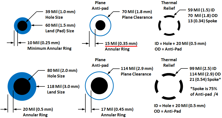
Conductor spacing and clearances further define layout integrity. Minimum land-to-land pitch for perpendicular mounting follows formulas like half body width plus lead span plus a spreading allowance, varying by level: 0.4 mm for A, 0.3 mm for B, and 0.2 mm for C. These prevent solder bridging in wave soldering while maximizing density. Hole location tolerances tighten with density, at 0.25 mm for level A, 0.20 mm for B, and 0.15 mm for C, aligning with drill accuracy. Electrical clearances between lands adhere to voltage-based minima, starting at 0.05 mm internal for low voltages, expanding for external uncoated surfaces.
Best Practices for Through-Hole Component Placement and Spacing
Effective through-hole component placement starts with logical grouping by function and soldering polarity to optimize wave flow. Align similar components in the same orientation, directing leads downstream relative to solder wave direction, which reduces shadowing and ensures even heating. Place high-profile components away from board edges, maintaining at least 5 mm from non-transmission edges and 10 mm from transmission edges to avoid warpage-induced stress. Polarized parts like electrolytic capacitors should follow consistent patterns for automated insertion, minimizing handling errors. Proximity to power and ground planes via nearby through-holes lowers inductance, enhancing signal integrity in mixed assemblies.
Through-hole component spacing must exceed minimum pitches to facilitate solder fillet formation and inspection. A courtyard excess around the land pattern—0.5 mm for level A, 0.25 mm for B, 0.1 mm for C—provides mechanical and electrical clearance from adjacent features. For wave soldering, maintain 1 mm minimum between through-hole pads to prevent bridging, adjusting for lead bending. Lead forming prior to insertion, with bends above the solder plane, reduces stress on pads and aids cleanup. Thermal relief patterns in power planes under lands mitigate solder theft, ensuring barrel fill exceeds 75% per class 2/3 criteria.
Design for manufacturability through-hole incorporates panelization and fiducial considerations, though less critical than for SMT. Separate drill charts for plated and non-plated holes streamline fabrication. Stand-off heights for cleaning, based on board diagonal and area, ensure flux residue evacuation—minimum 0.5 mm for small assemblies. Simulate solder flow in layout tools to verify joint quality, prioritizing J-STD-001 compliance for lead protrusion and wetting.
Troubleshooting Common Through-Hole Assembly Challenges
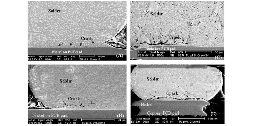
Engineers often encounter solder wicking into leads, depleting barrel fill; mitigate by precise hole-to-lead ratios and thermal spokes. Insufficient annular ring from misregistration causes breakout—counter with teardrop connections to traces. Bridging in dense areas stems from tight through-hole component spacing; widen pitches or use selective soldering for outliers. Lead protrusion exceeding 2.5 mm risks electrical spacing violations, addressed via controlled clinching. Post-assembly inspection per IPC-A-610 verifies fillet heights and hole fill, catching voids early.
Warpage affects multi-layer boards with asymmetric through-hole patterns; symmetrize placement and use support fixtures. For mixed THT/SMT, segregate zones to avoid reflow damage to through-hole parts.
Conclusion
Mastering design rules for through-hole assembly elevates PCB reliability and manufacturability. Key elements like through-hole pad size, hole size, component placement, and spacing interlink to form robust joints under IPC guidelines. By selecting appropriate density levels and applying best practices, engineers reduce defects and accelerate production. Prioritize simulation and DFM reviews to align layouts with process realities. These strategies ensure high-yield assemblies suited for demanding environments.
FAQs
Q1: What factors determine through-hole hole size in PCB design?
A1: Through-hole hole size is calculated as the maximum component lead diameter plus a clearance factor based on density level per IPC-7251. Level A adds 0.25 mm for robust insertion, B adds 0.20 mm, and C adds 0.15 mm to suit high-density needs. This ensures plating uniformity and ease of assembly while preventing lead damage. Always verify against component datasheets for tolerances.
Q2: How do you optimize through-hole pad size for reliability?
A2: Through-hole pad size follows IPC-2221A: finished hole diameter plus twice the annular ring plus fabrication allowance. Annular excesses are 0.50 mm (A), 0.35 mm (B), 0.30 mm (C), with allowances of 0.4 mm (A), 0.25 mm (B), 0.2 mm (C). This provides etchback margin and strong fillets. Larger pads enhance durability but consume space.
Q3: Why is through-hole component spacing critical for manufacturability?
A3: Through-hole component spacing prevents solder bridging and ensures inspection access during wave soldering. Minimum land pitches incorporate body width, lead span, and level-specific additions like 0.4 mm for A. Adequate spacing, around 1 mm pad-to-pad, supports flux flow and reduces defects. Group components to match conveyor direction.
Q4: What role does design for manufacturability through-hole play in mixed assemblies?
A4: Design for manufacturability through-hole integrates clearances for SMT coexistence, like zoning and thermal management. Orient leads for uniform wave exposure and maintain courtyard excesses for clearance. Compliance with J-STD-001 soldering criteria minimizes rework, boosting yield in hybrid boards.
References
IPC-2221A — Generic Standard on Printed Board Design. IPC, 2003
IPC-7251 — Generic Requirements for Through-Hole Design and Land Pattern Standard. IPC, 2008
J-STD-001G — Requirements for Soldered Electrical and Electronic Assemblies. IPC, 2017
IPC-A-610H — Acceptability of Electronic Assemblies. IPC, 2019