Introduction
In the realm of printed circuit board (PCB) design, component placement plays a pivotal role in ensuring efficient assembly, especially during batch production. For electrical engineers, optimizing board layout is not just about functionality but also about reducing assembly time and adhering to design for manufacturability (DFM) principles. A well planned component arrangement can minimize errors, lower production costs, and enhance reliability. This article delves into component placement guidelines tailored for batch assembly, focusing on practical strategies to streamline the process. By following these best practices, engineers can achieve an efficient PCB design that meets industry standards and supports high volume manufacturing needs. The insights provided here aim to bridge the gap between design intent and manufacturing reality, ensuring smooth transitions from prototype to production.
Why Component Placement Matters for Batch Assembly
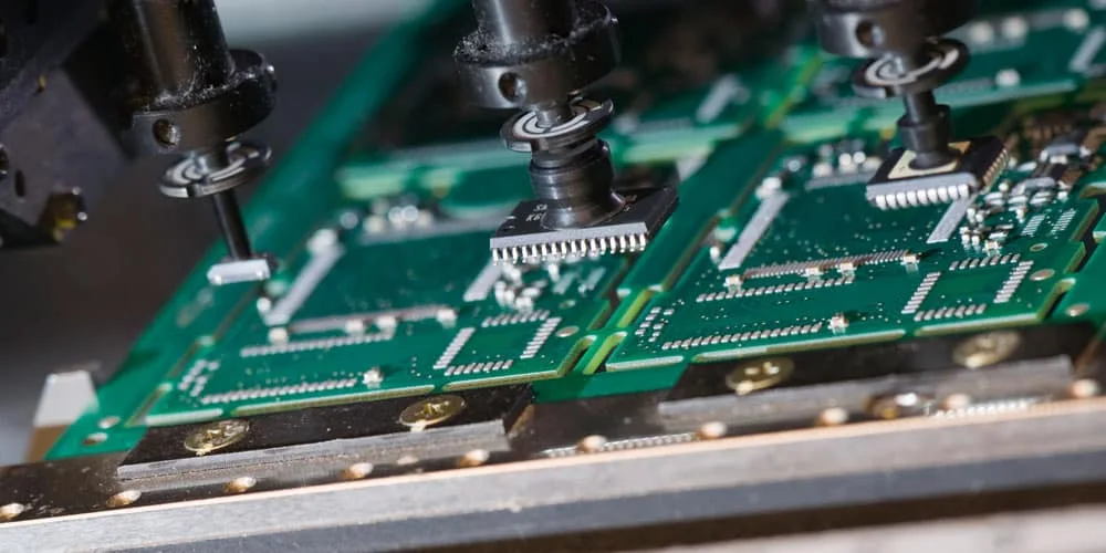
Component placement directly influences the efficiency of batch assembly processes. In high volume production, automated pick and place machines are used to position components quickly and accurately. Poor placement strategies can lead to increased assembly time, higher defect rates, and challenges in testing or rework. For instance, components placed too close together may cause issues with machine access or soldering quality. Additionally, improper orientation can disrupt the flow of automated assembly lines, causing delays. Adhering to DFM for batch assembly ensures that designs are compatible with manufacturing equipment capabilities and minimizes manual intervention. Ultimately, optimizing board layout through strategic placement reduces production bottlenecks, enhances yield, and ensures consistent quality across batches, which is critical for meeting project timelines and cost targets.
Technical Principles of Component Placement in Batch Assembly
Understanding the technical aspects of component placement is essential for achieving an efficient PCB design. The primary goal is to align the design with the capabilities of automated assembly systems while maintaining signal integrity and thermal performance. Below are key principles to consider.
Alignment with Pick and Place Machines
Automated assembly relies on pick and place machines that require components to be positioned in a predictable and accessible manner. Components must be oriented consistently, often following a uniform polarity or direction, to match the machine's programming. Spacing between components should comply with the machine's minimum clearance requirements to prevent collisions during placement or soldering.
Related Reading: The Essential Guide to Manual Pick and Place for Beginners
Grouping by Functionality and Size
Grouping components based on function or type can streamline assembly. For example, placing all surface mount resistors in one area allows the machine to use a single nozzle type, reducing tool changeovers. Similarly, taller components should be placed after smaller ones to avoid shadowing during soldering processes like reflow, which can impact thermal distribution.
Consideration for Signal Integrity
Placement also affects electrical performance. High speed signal components should be positioned close to their corresponding connectors or ICs to minimize trace lengths and reduce noise. Decoupling capacitors must be near power pins of integrated circuits to stabilize voltage. These arrangements prevent signal degradation and ensure reliable operation.
Related Reading: Component Placement Strategies for High Speed PCBs: Reducing EMI and Signal Loss
Thermal Management
Heat dissipation is another critical factor. Power dissipating components, such as voltage regulators, should be spaced adequately to avoid thermal hotspots. Placement near board edges or heat sinks can aid in cooling. Proper orientation can also facilitate airflow during operation, maintaining component longevity.
Best Practices for Component Placement in Batch Assembly
Implementing effective component placement guidelines can significantly enhance the efficiency of batch assembly. Below are actionable strategies for optimizing board layout and reducing assembly time.
Standardize Component Orientation
Ensure all components of the same type share a consistent orientation. For example, align diodes and capacitors with their polarity markers in the same direction. This uniformity simplifies programming for pick and place machines and reduces the risk of placement errors. Refer to industry standards like IPC-7351B for guidance on land pattern design and orientation.
Maintain Adequate Spacing
Adhere to minimum spacing rules between components to accommodate assembly equipment and soldering processes. Tight clustering can lead to solder bridging or insufficient access for rework. Standards such as IPC-2221B provide detailed recommendations on clearances based on component types and board density.
Prioritize Placement Sequence
Place critical components first, such as connectors and large ICs, to define the board's primary layout. Then, position smaller passive components around them. This hierarchical approach ensures stability during assembly and minimizes interference. It also aids in balancing the board for automated handling.
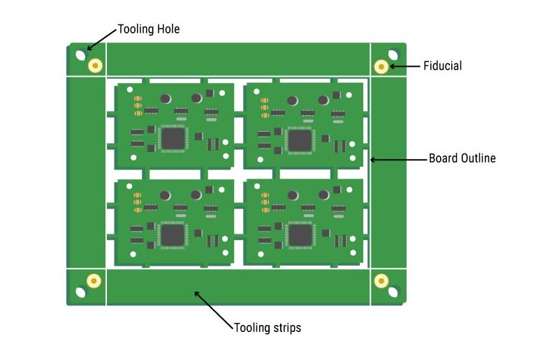
Optimize for Panelization
In batch assembly, multiple boards are often produced on a single panel. Design component placement to avoid interference with panel edges or breakaway tabs. Keep components away from areas designated for fiducial markers, which are essential for machine alignment during assembly.
Minimize Component Rotation
Limit the need for component rotation during placement. Ideally, components should be placed at 0 or 90 degree angles to align with standard machine capabilities. Non standard angles increase programming complexity and slow down the assembly process, impacting overall efficiency.
Related Reading: Mastering SMT Component Placement for Optimal PCB Design
Incorporate Test Points
Integrate test points in accessible locations to facilitate in circuit testing after assembly. Position these points away from densely populated areas to ensure probes can reach them without obstruction. This practice supports quality control without necessitating design revisions.
Account for Reflow and Wave Soldering
For designs using reflow soldering, ensure smaller components are not shadowed by taller ones to guarantee even heat distribution. In wave soldering, place through hole components on the bottom side with consistent orientation to match the wave direction, reducing defects like insufficient solder fill.
Addressing Common Challenges in Batch Assembly Placement
Even with careful planning, challenges can arise during batch assembly due to design oversights. One common issue is component misalignment caused by inconsistent silkscreen markings or fiducial inaccuracies. To mitigate this, ensure fiducials are placed in clear, unobstructed areas as per IPC-7351B guidelines. Another challenge is thermal imbalance during soldering, often due to uneven component distribution. Spread out heat generating components and verify thermal profiles against standards like IPC-7530A for reflow processes. Additionally, high density designs may lead to pick and place errors if spacing is inadequate. Review designs against IPC-2221B clearance rules to avoid such risks. Addressing these issues during the design phase prevents costly rework and ensures smooth production runs.
Conclusion
Effective component placement is a cornerstone of successful batch assembly in PCB production. By adhering to well established guidelines and prioritizing DFM for batch assembly, electrical engineers can create designs that optimize board layout and reduce assembly time. Consistent orientation, adequate spacing, and strategic sequencing are just a few practices that enhance manufacturing efficiency. Aligning designs with industry standards ensures compatibility with automated systems and minimizes production errors. As batch assembly demands precision and scalability, investing time in placement planning yields significant returns in cost savings and product reliability. These best practices empower engineers to bridge design and manufacturing, delivering high quality PCBs that meet stringent performance criteria.
FAQs
Q1: What are the key component placement guidelines for batch assembly?
A1: Component placement guidelines for batch assembly focus on consistency and accessibility. Orient components uniformly, maintain adequate spacing per IPC-2221B standards, and prioritize critical parts like connectors first. Group similar components to minimize tool changes in pick and place machines. Ensure test points are accessible and avoid panel edge interference. These steps streamline production, reduce errors, and support efficient PCB design for high volume manufacturing.
Q2: How does optimizing board layout reduce assembly time?
A2: Optimizing board layout reduces assembly time by aligning the design with automated equipment capabilities. Uniform component orientation and logical grouping minimize machine reprogramming and tool swaps. Adequate spacing prevents placement errors, while strategic sequencing ensures smooth operation. Following DFM for batch assembly principles, such as those in IPC-7351B, cuts down on manual adjustments, speeding up the process and enhancing overall production efficiency.
Q3: Why is DFM for batch assembly critical in PCB design?
A3: DFM for batch assembly is vital as it ensures PCB designs are compatible with manufacturing processes. It focuses on practical placement and layout to avoid production bottlenecks. By adhering to standards like IPC-2221B, engineers prevent issues like component interference or soldering defects. This approach lowers costs, improves yield, and ensures scalability, making it a cornerstone of efficient PCB design for large scale production.
Q4: What standards support efficient PCB design for batch assembly?
A4: Efficient PCB design for batch assembly relies on widely recognized standards. IPC-7351B provides guidelines for land patterns and orientation. IPC-2221B outlines clearance and spacing requirements to prevent assembly issues. IPC-7530A offers insights into thermal profiles for soldering processes. These standards ensure designs are manufacturable, reduce assembly time, and maintain quality across batches, supporting reliable production outcomes.
References
IPC-7351B — Generic Requirements for Surface Mount Design and Land Pattern Standard. IPC, 2010.
IPC-2221B — Generic Standard on Printed Board Design. IPC, 2012.
IPC-7530A — Guidelines for Temperature Profiling for Mass Soldering Processes (Reflow & Wave). IPC, 2017.


