Introduction
Assembling surface-mount PCBs at home often challenges hobbyists with precise solder paste application. Professional stencils ensure uniform deposits, but their cost can deter small runs or prototypes. DIY solder paste stencils offer low-cost alternatives using accessible tools and materials. This guide covers homemade stencil methods, from etching solder stencils to laser cutting stencils, tailored for electronic hobbyists. You will learn practical steps, troubleshooting tips, and best practices to achieve reliable results without factory equipment. These techniques align with core principles for consistent PCB assembly.

What Is a Solder Paste Stencil and Why It Matters
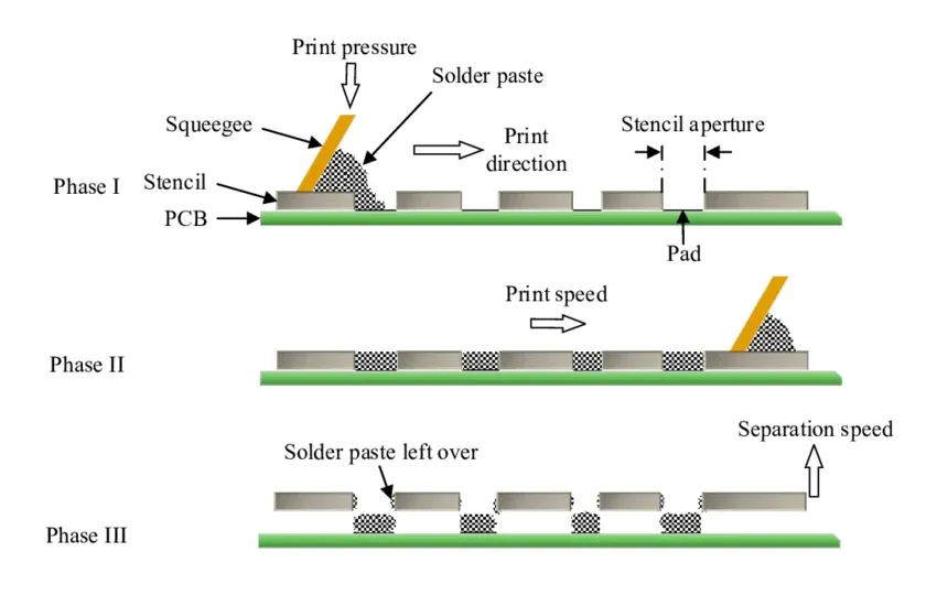
A solder paste stencil is a thin sheet, typically metal or polymer, with precisely cut apertures matching PCB pad layouts. During assembly, it aligns over the board, allowing solder paste to transfer only to pads when squeegeed across. This method prevents excess paste that causes bridging or insufficient volume leading to weak joints. For hobbyists, it simplifies surface-mount technology (SMT) processes otherwise reliant on manual dispensing. Consistent paste volume directly impacts reflow soldering quality and joint reliability.
In low-volume production, stencils reduce defects compared to hand-soldering or syringe methods. They enable repeatable prints across multiple boards, saving time on prototypes. Poor stencil design often results in uneven deposits, tombstoning, or voids, complicating troubleshooting. Industry guidelines like IPC-7525C emphasize aperture shapes and spacing to optimize paste release. Hobbyists benefit from these principles to mimic professional outcomes affordably.
Technical Principles of Solder Paste Stencils
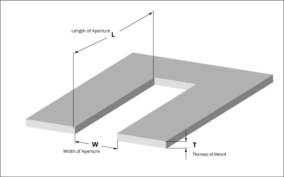
Stencil performance hinges on material properties, aperture geometry, and printing dynamics. Metals like stainless steel or brass provide durability for repeated use, while polymers suit one-off jobs due to lower cost. Aperture walls must be smooth to allow clean paste release, avoiding stringing or residue. The area ratio, defined as (aperture area divided by perimeter times thickness), influences release efficiency. Standards such as IPC-7525C recommend designs promoting ratios above critical thresholds for reliable printing.
Paste transfer efficiency depends on stencil thickness relative to pad size. Thinner stencils work for fine-pitch components, reducing paste volume and bridging risk. Conversely, thicker ones suit larger pads needing more solder. Alignment tolerances must match board fiducials or edges for accuracy. During printing, squeegee pressure and speed control deposit uniformity across the board.
Surface tension in solder paste plays a key role post-lift-off. Flux activators aid clean separation from aperture walls. Environmental factors like humidity affect paste rheology, potentially causing smearing. Testing prints on scrap boards verifies design before full assembly.
Homemade Stencil Methods for Low-Cost Assembly
Hobbyists have several DIY solder paste stencil options, each balancing cost, precision, and tool access. Chemical etching solder stencils uses photoresist-coated foil for detailed apertures. Laser cutting stencils leverages desktop cutters for polymer sheets. Other low-cost stencil alternatives include plotter-cut films or improvised materials. Selection depends on your setup, board complexity, and pitch size.
Chemical Etching Solder Stencils
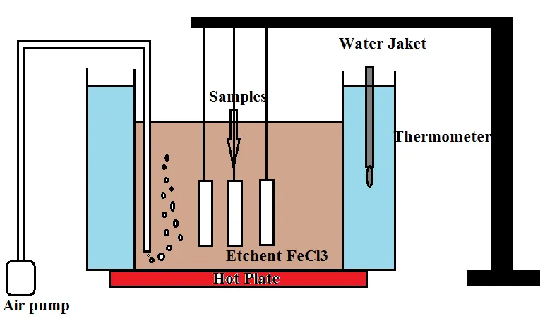
Etching starts with thin brass or copper shim stock, typically sourced from hardware suppliers. Apply photoresist film or liquid to one side, then expose using a printed transparency mask under UV light. Develop the resist to reveal pad patterns, then immerse in ferric chloride etchant. Agitate gently until apertures clear, rinse thoroughly, and strip remaining resist. This method yields metal stencils durable for dozens of prints.
Troubleshoot over-etching by timing baths precisely and using fresh etchant. Under-etching leaves burrs, requiring light sanding for smooth walls. Mask alignment ensures pad fidelity. Etched stencils excel for fine-pitch up to 0.4mm but demand darkroom basics.
Laser Cutting Stencils
Desktop CO2 or diode lasers cut apertures into mylar, kapton, or polycarbonate sheets. Export Gerber paste layers from your PCB design software as vector files for the laser controller. Secure the sheet in the machine, focus the beam, and run multiple passes for clean through-cuts. Post-process by cleaning debris and mounting on a frame with adhesive tape. Laser stencils suit quick prototypes, offering sub-millimeter precision.
Adjust power and speed to avoid melting edges, which trap paste. Thinner sheets under 0.1mm prevent bridging on dense boards. Test cuts on scrap material first. This approach shines for irregular shapes or revisions without chemicals.

Other Low-Cost Stencil Alternatives
Vinyl cutters produce temporary stencils from adhesive-backed film, ideal for coarse pitches. Plotter-cut mylar withstands a few prints if squeegeed carefully. Improvised options like soda can aluminum, laser-etched, work for tiny boards but lack uniformity. 3D-printed stencils with soluble supports offer novelty but suffer poor release. Hand-cut frisket film serves emergencies, though alignment proves tricky.
Compare methods by durability and resolution: etching for metal longevity, laser for speed. Hybrid approaches, like etching frames holding laser-cut foils, extend usability.
Practical Solutions and Best Practices
Frame your stencil tautly using embroidery hoops or wooden clamps to prevent flexing during printing. Align visually or with pins matching board holes. Choose Type 3 or 4 solder paste for hobby reflow ovens, storing it refrigerated. Apply paste with a plastic squeegee at 45 degrees, moderate pressure, and steady speed. Lift the stencil perpendicularly to minimize smearing.
Clean stencils post-use with isopropyl alcohol and lint-free wipes, avoiding abrasives. Inspect apertures under magnification for buildup. For multi-layer pastes, print bottom side first if needed. J-STD-001 guidelines stress uniform deposits for acceptable joints.
Troubleshooting Common Issues
Insufficient paste volume causes open joints; enlarge apertures slightly or thin the stencil. Bridging arises from excess paste or poor release; refine area ratios per IPC-7525C. Smearing indicates dirty surfaces or high humidity; dry boards and control environment. Uneven prints signal warped stencils; flatten with weights.
Reflow inspection reveals voids from trapped air; agitate paste before printing. Iterative testing refines your process.
Conclusion
DIY solder paste stencils empower hobbyists to assemble professional-grade PCBs affordably. Methods like etching solder stencils and laser cutting stencils provide flexible low-cost stencil alternatives tailored to home setups. Adhering to principles from IPC-7525C ensures reliable paste transfer and joint quality. Practice troubleshooting elevates results, bridging the gap to production standards. Experiment safely, iterate designs, and enjoy precise SMT assembly without high costs.
FAQs
Q1: How do I make a DIY solder paste stencil at home?
A1: Start with brass shim for etching or mylar for laser cutting. For etching, apply photoresist, expose with a mask, develop, and etch in ferric chloride. Laser methods use Gerber files on a desktop cutter for quick apertures. Mount on a rigid frame, test alignment, and verify prints on scrap PCBs. This homemade stencil method cuts costs while maintaining precision for hobby projects.
Q2: What are the pros and cons of etching solder stencils versus laser cutting stencils?
A2: Etching produces durable metal stencils for repeated use but involves chemicals and drying time. Laser cutting stencils offers speed and no wet processes, ideal for prototypes, though polymers wear faster. Both achieve fine features, but etching suits complex boards per IPC guidelines. Choose based on tools: etching for darkroom access, laser for digital workflows. Troubleshoot edges for optimal release.
Q3: Are low-cost stencil alternatives reliable for fine-pitch components?
A3: Vinyl or mylar plotter cuts work for pitches above 0.65mm but struggle with 0.4mm due to tear risk. Laser-cut polymers handle finer pitches reliably if walls are crisp. Always test paste volume and reflow. Avoid hand-cutting for density; prioritize smooth apertures. These alternatives enable hobby SMT without compromising basic joint integrity.
Q4: How can I troubleshoot poor solder paste release from a DIY stencil?
A4: Clean apertures thoroughly and ensure smooth walls by sanding burrs. Optimize squeegee angle and speed for even pressure. Use fresh paste with good flux activity. Check area ratios aligning with IPC-7525C for better release. Humidity control prevents sticking. Iterative scrap prints refine technique effectively.
References
IPC-7525C — Stencil Design Guidelines. IPC, 2021
J-STD-001GS — Requirements for Soldered Electrical and Electronic Assemblies. IPC, 2020
IPC-A-610H — Acceptability of Electronic Assemblies. IPC, 2019