Introduction
In the design of multi-layer printed circuit boards (PCBs), managing noise is a critical challenge for ensuring reliable performance. High-speed circuits and dense component layouts often lead to power supply fluctuations and electromagnetic interference, which degrade signal integrity. Decoupling capacitors and bypass capacitors play a vital role in stabilizing the power distribution network (PDN) and achieving effective noise reduction. For electrical engineers, understanding how to implement these components in a multi-layer PCB is essential to maintain system stability and prevent issues like ground bounce or crosstalk. This article explores the principles behind decoupling techniques, practical strategies for implementation, and best practices to optimize signal integrity. By focusing on proven methods, we aim to provide actionable insights for designing robust PCB layouts that minimize noise.
What Are Decoupling Techniques and Why Do They Matter?
Decoupling techniques involve the strategic use of capacitors to isolate or filter noise in the power supply lines of a PCB. Specifically, decoupling capacitors and bypass capacitors are placed between power and ground planes to provide a local reservoir of charge. This setup ensures that sudden current demands from active components do not cause voltage drops in the PDN. In multi-layer PCBs, where high-speed signals and multiple power domains coexist, noise reduction is crucial to prevent interference and maintain signal integrity.
The importance of these techniques cannot be overstated. Without proper decoupling, transient currents can induce noise, leading to erratic behavior in digital circuits or analog signal distortion. For engineers working on complex designs, such as those in telecommunications or automotive systems, mastering decoupling is a fundamental step to achieving reliable operation and meeting stringent performance standards.
Technical Principles of Decoupling in Multi-Layer PCBs
Understanding Noise in Power Distribution Networks
Noise in a PDN arises from various sources, including switching transients of integrated circuits, parasitic inductance in traces, and electromagnetic coupling between layers. In multi-layer PCBs, the close proximity of power and ground planes helps reduce loop inductance, but it does not eliminate noise entirely. When a component draws a sudden burst of current, the voltage across the PDN can fluctuate if the power supply cannot respond quickly enough. This phenomenon, often termed as power supply ripple, directly impacts signal integrity.
Role of Decoupling and Bypass Capacitors
Decoupling capacitors act as local energy storage units, supplying instantaneous current to components during high-frequency switching. They are typically placed near the power pins of active devices to minimize the impedance path. Bypass capacitors, often used interchangeably with decoupling capacitors in this context, serve a similar purpose by shunting high-frequency noise to ground. The effectiveness of these capacitors depends on their value, type, and placement within the PCB layout.
Impedance and Resonance Considerations
The primary goal of decoupling is to maintain low impedance across a wide frequency range in the PDN. Capacitors of different values are often combined to cover various frequency bands. For instance, larger capacitors handle low-frequency noise, while smaller ones address high-frequency disturbances. However, engineers must also consider resonance effects, where the interaction between capacitors and parasitic inductance can create impedance peaks at specific frequencies. Careful selection and placement are necessary to avoid such issues.
Practical Solutions for Effective Decoupling in Multi-Layer PCBs
Selecting the Right Capacitor Values and Types
Choosing appropriate capacitor values is a critical step in noise reduction. A common practice is to use a combination of capacitors with values spanning several orders of magnitude, such as 0.1 microfarads, 1 microfarad, and 10 microfarads. This approach ensures coverage across a broad spectrum of frequencies. Ceramic capacitors are often preferred for high-frequency decoupling due to their low equivalent series resistance and inductance. Electrolytic or tantalum capacitors may be used for bulk capacitance at lower frequencies.
Optimal Placement of Decoupling Capacitors
Placement directly impacts the performance of decoupling capacitors. To minimize inductance, capacitors should be positioned as close as possible to the power pins of the target component. In multi-layer PCBs, vias connecting to power and ground planes must be short and direct. Engineers should prioritize placing smaller value capacitors closest to the pins for high-frequency noise, while larger capacitors can be slightly farther away for bulk energy storage.
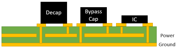
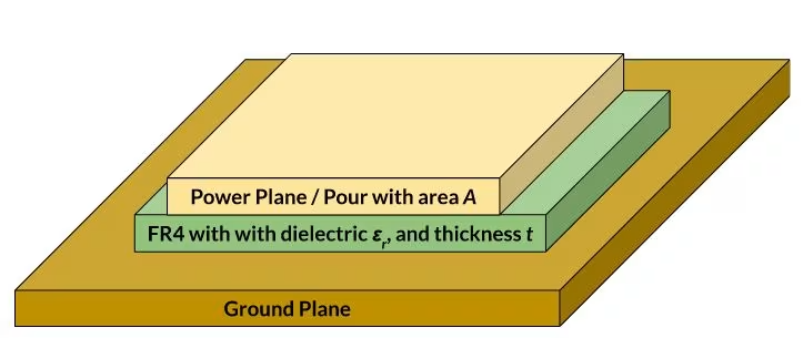
Layer Stack-Up Design for Enhanced Decoupling
The stack-up design of a multi-layer PCB significantly influences the effectiveness of the PDN. Placing power and ground planes adjacent to each other reduces loop inductance and enhances the natural capacitance between planes. This inherent capacitance acts as an additional decoupling mechanism, complementing discrete capacitors. Engineers should aim for thin dielectric layers between power and ground planes to maximize this effect, adhering to guidelines outlined in industry standards like IPC-2221B for generic PCB design.
Multiple Capacitor Networks for Broad Frequency Coverage
Using multiple capacitors in parallel is a widely accepted practice to achieve low impedance over a wide frequency range. However, care must be taken to avoid anti-resonance effects, where the combined impedance of capacitors peaks at certain frequencies. Simulation tools compliant with standards such as IPC-D-317A can help predict and mitigate these issues during the design phase.
Ground Plane Integrity and Via Placement
A solid ground plane is essential for effective noise reduction. Splitting ground planes or introducing gaps can create return path discontinuities, exacerbating noise and degrading signal integrity. Vias used for connecting decoupling capacitors to ground and power planes must be placed to minimize path length. Multiple vias can be used for high-current paths to reduce inductance and improve current-carrying capacity.
Related Reading: Power Plane Decoupling: A Comprehensive Guide to PCB Stability
Troubleshooting Common Decoupling Challenges
Identifying Insufficient Decoupling
Inadequate decoupling often manifests as voltage ripples or unexpected glitches in circuit operation. Engineers can use oscilloscopes to measure power supply noise at the pins of active components. If significant fluctuations are observed during switching events, additional capacitors or better placement may be required. Simulation during the design phase, following guidelines from standards like IPC-2141A for controlled impedance, can prevent such issues.
Addressing High-Frequency Noise
High-frequency noise often results from improper capacitor selection or placement. If smaller value capacitors are not close enough to the component pins, their effectiveness diminishes due to increased inductance. Reviewing the layout and ensuring minimal distance between capacitors and pins is a practical solution. Using capacitors with low equivalent series inductance is also beneficial.
Related Reading: PCB Grounding Techniques: A Guide to Minimizing Noise and Ensuring Reliable Connections
Mitigating Resonance and Impedance Peaks
Resonance in the PDN can lead to unexpected noise amplification at specific frequencies. This issue often arises when multiple capacitors are used without considering their interaction with parasitic elements. Engineers can address this by staggering capacitor values and using damping techniques, such as adding small series resistors to larger capacitors, to suppress resonance peaks.
Conclusion
Effective decoupling techniques are indispensable for achieving noise reduction in multi-layer PCBs. By understanding the principles of decoupling capacitors and bypass capacitors, engineers can design robust power distribution networks that ensure signal integrity. Strategic capacitor selection, optimal placement, and careful layer stack-up design are key to minimizing noise and preventing performance issues. Adhering to established industry standards and employing simulation tools during the design process further enhances reliability. As PCB designs continue to grow in complexity, mastering these techniques will remain a cornerstone of successful electronic system development.
FAQs
Q1: How do decoupling capacitors improve signal integrity in multi-layer PCBs?
A1: Decoupling capacitors stabilize the voltage supply by providing local charge during sudden current demands, thus reducing noise in the power distribution network. Positioned near component pins, they minimize voltage fluctuations that could disrupt signal integrity. This ensures consistent performance of high-speed circuits, preventing issues like crosstalk or timing errors in complex multi-layer PCB designs.
Q2: What is the difference between decoupling capacitors and bypass capacitors for noise reduction?
A2: Decoupling capacitors and bypass capacitors are often used interchangeably, but their roles can differ slightly. Decoupling capacitors focus on isolating noise in the power supply, while bypass capacitors shunt high-frequency noise to ground. Both contribute to noise reduction in multi-layer PCBs, ensuring a stable power distribution network and protecting sensitive components from interference.
Q3: How does the power distribution network affect noise in multi-layer PCBs?
A3: The power distribution network (PDN) directly influences noise levels in multi-layer PCBs. A poorly designed PDN with high impedance or long current paths can amplify voltage fluctuations and electromagnetic interference. Proper PDN design, incorporating decoupling capacitors and solid ground planes, minimizes noise, ensuring stable power delivery and maintaining signal integrity across layers.
Q4: What are the best practices for capacitor placement in multi-layer PCB designs?
A4: For optimal noise reduction, place decoupling capacitors as close as possible to the power pins of active components in multi-layer PCB designs. Use short, direct vias to connect to power and ground planes. Prioritize smaller capacitors for high-frequency noise near pins, and larger ones for bulk capacitance slightly farther, ensuring minimal inductance and effective filtering.
References
IPC-2221B — Generic Standard on Printed Board Design. IPC, 2012.
IPC-2141A — Design Guide for High-Speed Controlled Impedance Circuit Boards. IPC, 2004.
IPC-D-317A — Design Guidelines for Electronic Packaging Utilizing High-Speed Techniques. IPC, 1995.


