Introduction
Signal integrity refers to the preservation of signal quality as it travels through a printed circuit board in high-speed designs. In modern electronics, where data rates exceed several gigabits per second, maintaining clean signals prevents errors, data corruption, and system failures. High-speed PCB designs face challenges from reflections, crosstalk, and noise, which degrade performance if not addressed early. Engineers must integrate signal integrity considerations from the initial layout stage to ensure reliable operation. This article explores proven strategies to enhance signal integrity, focusing on critical elements like impedance control, trace routing, termination techniques, ground planes, and decoupling capacitors. By applying these principles, designers achieve robust boards that meet demanding performance requirements.
Understanding Signal Integrity in High-Speed PCB Designs
Signal integrity encompasses the electrical characteristics that ensure signals arrive at their destination with intended shape, timing, and amplitude. In high-speed environments, signals behave as transmission lines where wavelength approaches trace lengths, leading to phenomena like ringing and overshoot. Poor signal integrity manifests as bit errors, timing skew, or electromagnetic interference, compromising overall system reliability. Engineers evaluate signal integrity through time-domain reflectometry and eye diagram analysis during validation. Adhering to established design guidelines minimizes these issues from the outset. Ultimately, strong signal integrity supports higher clock speeds and denser integrations in applications from telecommunications to computing.
Key Challenges Affecting Signal Integrity
High-speed signals encounter impedance mismatches that cause reflections, distorting waveforms and introducing jitter. Crosstalk occurs when adjacent traces couple energy, injecting noise into sensitive lines. Ground bounce and power supply noise further exacerbate issues by creating return path discontinuities. Dielectric losses and skin effect attenuate high-frequency components, reducing signal amplitude over distance. Vias and bends introduce discontinuities that alter characteristic impedance. Addressing these challenges requires a holistic approach combining layout optimization and component placement.
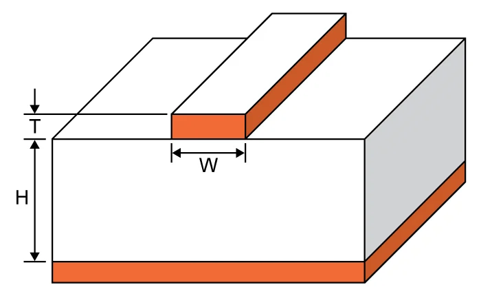
Implementing Impedance Control for Reliable Transmission
Impedance control maintains consistent characteristic impedance along signal paths, preventing reflections at transitions. Designers calculate trace width, spacing, and layer stackup to achieve target values, typically using microstrip or stripline configurations. As detailed in IPC-2141, guidelines for high-speed controlled impedance circuit boards emphasize precise geometry and material properties. Fabricators verify impedance through time-domain reflectometry post-manufacture to confirm tolerances. Selecting low-loss dielectrics further supports broadband performance. Proper impedance control forms the foundation for clean signal propagation in multilayer boards.
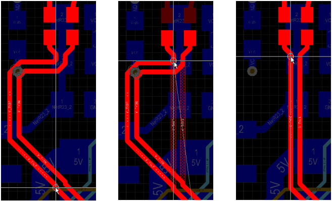
Optimized Trace Routing Techniques
Trace routing dictates signal path integrity by minimizing length variations and discontinuities. Differential pairs require symmetric routing to preserve balance and reduce common-mode noise. Avoid right-angle bends, opting for 45-degree or curved transitions to reduce reflections. Route high-speed traces over continuous reference planes to stabilize return currents. Length matching ensures simultaneous arrival for clock-to-data relationships. Segregate analog and digital signals to limit crosstalk coupling.
In multilayer boards, dedicate inner layers for high-speed routing adjacent to ground planes. Minimize via usage by planning component placement strategically. These practices align with general design standards like IPC-2221 for printed board layouts. Controlled spacing between traces further mitigates near-end and far-end crosstalk.
Termination Techniques to Eliminate Reflections
Termination techniques match line impedance at endpoints, absorbing signals without reflection. Series termination places a resistor near the driver to dampen edges, suitable for point-to-point connections. Parallel termination at the receiver provides low-impedance matching but consumes more power. AC termination uses a resistor-capacitor network to minimize DC loading while controlling reflections. Thevenin termination combines resistors for precise matching across voltage swings. Selection depends on topology, speed, and power budget.
Engineers simulate termination schemes to optimize resistor values and positions. For buses, daisy-chain or star topologies influence termination strategy. Proper implementation ensures flat eye openings and low bit error rates. These methods prove essential in multi-drop environments where multiple reflections compound.
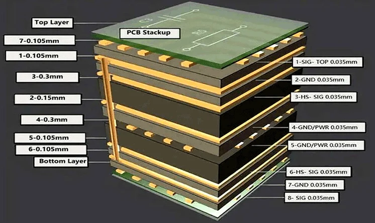
Leveraging Ground Planes for Return Path Stability
Ground planes provide low-inductance return paths, confining fields and reducing loop inductance. A solid ground plane beneath signal traces maintains reference for impedance calculations and shields against crosstalk. Split planes demand stitching vias to preserve current flow continuity. Power planes complement ground planes but require decoupling to isolate noise. In high-speed designs, adjacent ground and power plane pairs form stripline structures with superior confinement.
Voids in ground planes create impedance bumps, so fill them with stitching capacitors or vias. Multiple ground planes distribute return currents effectively in dense layouts. Ground planes also aid thermal dissipation and EMI suppression. Consistent ground plane usage enhances overall signal integrity margins.
Strategic Placement of Decoupling Capacitors
Decoupling capacitors shunt high-frequency noise from power rails to ground, stabilizing supply voltages for ICs. Place capacitors as close as possible to power pins, ideally within millimeters, to minimize loop inductance. Use a combination of ceramic values for broad-spectrum filtering, from bulk electrolytics to low-ESR 0.1uF units. Via-in-pad configurations reduce parasitics in high-density boards. Decoupling effectiveness depends on board thickness and plane proximity.
Integrate decoupling into power distribution network analysis for optimal coverage. Arrays of capacitors around high-current ICs handle transient demands. Poor placement leads to ground bounce impacting signal integrity. Systematic decoupling complements ground planes for quiet power delivery.
Integrating Best Practices for Comprehensive Signal Integrity
Combine impedance control with meticulous trace routing to form lossless transmission lines. Termination techniques pair with ground planes to manage reflections and returns. Decoupling capacitors ensure clean power, mitigating noise coupling into signals. Simulate the full stackup early to predict behaviors and iterate layouts. Post-layout verification through hyperlynx or similar confirms margins before fabrication. Compliance with performance specifications like IPC-6012E ensures manufacturability and reliability.
Conclusion
Enhancing signal integrity in high-speed PCB designs demands disciplined application of impedance control, trace routing, termination techniques, ground planes, and decoupling capacitors. These elements interlink to combat reflections, crosstalk, and noise effectively. Logical planning and structured verification yield boards that perform reliably at multi-Gbps speeds. Engineers benefit from referencing core standards to guide decisions. Prioritizing these practices reduces iterations and accelerates time-to-market. Robust signal integrity elevates design quality across demanding applications.
FAQs
Q1: How does impedance control impact high-speed PCB performance?
A1: Impedance control ensures characteristic impedance matches along traces, minimizing reflections that distort signals. In high-speed designs, mismatches cause ringing and jitter, degrading eye diagrams. Designers specify stackup parameters for 50-ohm single-ended or 100-ohm differential targets. Verification during fabrication confirms consistency, aligning with guidelines in IPC-2141. This practice sustains data rates beyond 10 Gbps reliably.
Q2: What are essential trace routing strategies for signal integrity?
A2: Prioritize short, direct paths with length matching for differential pairs to avoid skew. Route over solid ground planes and use 45-degree bends to reduce discontinuities. Maintain adequate spacing to suppress crosstalk. Symmetric routing preserves balance in pairs. These techniques, supported by IPC-2221 principles, enhance overall signal quality in multilayer boards.
Q3: Why are termination techniques critical in high-speed designs?
A3: Termination prevents signal reflections by matching impedances at endpoints, ensuring clean edges. Series or parallel methods suit different topologies, absorbing energy effectively. Without termination, multi-reflections accumulate, causing overshoot and EMI. Selection considers driver strength and line length. Proper application widens timing margins for high data rates.
Q4: How do ground planes and decoupling capacitors work together?
A4: Ground planes offer low-impedance returns, while decoupling capacitors filter noise on power lines. Place capacitors near IC pins over planes to form tight loops. This duo reduces ground bounce and supply ripple coupling into signals. Continuous planes with stitching maintain integrity. Together, they stabilize the entire PDN for superior performance.
References
IPC-2141A — Design Guide for High-Speed Controlled Impedance Circuit Boards. IPC, 1996
IPC-2221B — Generic Standard on Printed Board Design. IPC, 2003
IPC-6012E — Qualification and Performance Specification for Rigid Printed Boards. IPC, 2017


