Introduction
In electronics manufacturing, quality control processes ensure that printed circuit boards meet stringent reliability standards. Automated Optical Inspection, or AOI, has long served as a frontline tool for detecting visible defects during surface mount technology assembly. However, as components become smaller and more densely packed, hidden defects pose significant risks that AOI cannot address. This is where Automated X-ray Inspection, or AXI, steps in, providing visibility into obscured areas like solder joints under ball grid array packages. Understanding the shift from AOI to AXI highlights why x-ray inspection is essential for achieving zero-defect production in modern electronics manufacturing. Factory engineers increasingly integrate both methods to balance speed and thoroughness.
Understanding Automated Optical Inspection (AOI)
AOI employs high-resolution cameras and structured light to capture images of the PCB surface after key assembly stages, such as solder paste printing, component placement, and reflow soldering. Software algorithms compare these images against a golden sample or CAD data to identify anomalies like missing parts, misalignment, or solder bridges. This method excels in high-speed lines where rapid feedback prevents defects from propagating. It operates non-destructively, allowing real-time adjustments in the production flow. Despite its efficiency, AOI remains limited to line-of-sight inspections, missing subsurface issues common in advanced packages.
What Is Automated X-Ray Inspection (AXI)?
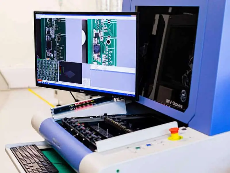
Automated x-ray inspection uses a controlled x-ray source to penetrate components and boards, generating radiographic images that reveal internal structures. A detector captures the transmitted x-rays, and advanced image processing software analyzes density variations to detect defects. In PCB assembly, AXI targets hidden solder joints in components like BGAs, QFNs, and chip-scale packages, where optical methods fail. The process integrates seamlessly into inline systems, scanning boards as they move through the production line. Operators program inspection recipes based on component libraries, ensuring consistent evaluation across batches. This technology aligns with factory needs for non-destructive, high-resolution quality assurance.
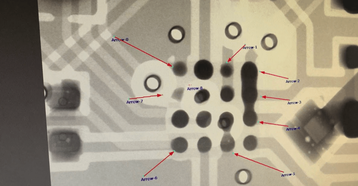
The x-ray inspection process begins with board positioning under the x-ray tube, followed by exposure to low-energy x-rays that differentiate materials by atomic density. Software reconstructs 2D or 3D images, flagging issues such as voids, cracks, or insufficient fillet formation. Tilt or oblique-angle imaging enhances accuracy for multi-layer boards. Post-inspection, data logs support process optimization and traceability. Factories calibrate systems regularly to maintain image quality and minimize false calls.
AOI vs AXI: Key Differences in Defect Detection
When comparing AOI vs AXI, the primary distinction lies in penetration capability; AOI relies on visible light for surface-level checks, while AXI penetrates opaque materials to inspect hidden features. AOI quickly verifies component presence, polarity, and gross soldering errors but overlooks voids in BGA balls or bridging beneath packages. AXI complements this by quantifying solder volume, head-in-pillow defects, and tombstoning in obscured joints, critical for high-reliability applications. Production speed favors AOI for high-volume runs, whereas AXI's slower scan times suit targeted post-reflow verification. Integrating both maximizes coverage, with AOI handling 80-90% of defects and AXI addressing the rest.
In terms of setup, AOI programming draws from Gerber files for fast implementation, while AXI requires component-specific profiles to interpret grayscale densities accurately. Cost considerations also differ; AOI systems offer lower upfront investment for broad screening, but AXI delivers superior return through reduced field failures. Factories often deploy AOI pre-reflow and AXI post-reflow for layered assurance. This hybrid approach aligns with standards like IPC-A-610, which define acceptability criteria for visible and hidden solder joints.
The X-Ray Inspection Process in Detail
The automated x-ray inspection process starts with conveyor-fed board handling, ensuring precise alignment for repeatable imaging. An x-ray generator emits a fan-shaped beam, modulated for optimal contrast between solder, copper, and silicon. Detectors, often linear arrays, convert x-rays to digital signals, producing real-time tomograms. Software applies filters to enhance edges and measure joint metrics against thresholds derived from design rules. Defects trigger alarms, diverting boards for rework while passing others downstream.
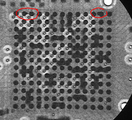
Advanced AXI variants incorporate computed tomography for 3D reconstruction, slicing through assemblies to visualize layer-by-layer integrity. Tilt mechanisms allow multi-angle views, crucial for detecting slant-induced shadows in dense BGAs. Data output includes defect maps and statistical process control charts, aiding yield analysis. Operators validate calls through magnified review stations, minimizing operator dependency. This methodical workflow supports electronics manufacturing scalability from prototypes to mass production.
X-Ray Inspection Benefits in Electronics Manufacturing
X-ray inspection benefits include unparalleled detection of latent defects that compromise long-term reliability, such as micro-voids exceeding acceptable limits in high-current joints. In modern electronics manufacturing, where miniaturization drives BGA and QFN adoption, AXI prevents escapes that AOI misses, reducing warranty costs. It enables process fine-tuning, like reflow profile adjustments based on void statistics, boosting first-pass yields. Non-destructive nature preserves boards for functional testing, unlike cross-sectioning. Factories gain traceability with archived images, supporting audits per IPC J-STD-001 soldering requirements.
Beyond defect detection, automated x-ray inspection fosters material verification, confirming wire bonding integrity or die attach quality in packages. It scales with complexity, handling fine-pitch arrays down to 0.3mm without resolution loss. Integration with manufacturing execution systems provides real-time dashboards, correlating inspections to upstream variables like stencil wear. These advantages position AXI as indispensable for automotive, aerospace, and medical sectors demanding zero-failure tolerance.
Best Practices for Implementing AXI
Select AXI systems with oblique imaging and high-resolution detectors matched to your smallest pitch. Develop inspection programs collaboratively with process engineers, validating against known good boards. Schedule routine calibration using phantoms to ensure grayscale accuracy. Combine AXI with AOI and SPI for comprehensive coverage, sequencing post-placement AOI, post-reflow AXI, and final ICT. Train operators on interpretation per IPC-A-610 classes, emphasizing void criteria for class 3 assemblies.
Monitor false call rates, adjusting algorithms iteratively from production data. Maintain x-ray safety protocols, including shielding and dosimetry. For high-mix lines, leverage offline programming to minimize downtime. Archive results for trend analysis, correlating defects to supplier lots or oven profiles. These practices embed AXI into factory workflows, enhancing overall quality control.
Conclusion
Transitioning from AOI to AXI addresses the visibility gap in complex electronics manufacturing, ensuring hidden defects do not undermine product reliability. While AOI provides efficient surface checks, AXI's subsurface insights are vital for advanced packages and dense boards. The x-ray inspection process, with its rigorous analysis, delivers actionable data for process refinement. Benefits extend to yield improvement and compliance with key standards. Engineers should prioritize hybrid inspection strategies to meet evolving demands. Ultimately, AXI solidifies quality foundations in high-stakes production environments.
FAQs
Q1: What is the main difference between AOI and AXI in PCB inspection?
A1: AOI uses optical imaging for surface defects like component misalignment, while AXI employs x-rays to reveal hidden solder issues in BGAs and QFNs. AOI suits high-speed screening, but AXI excels in AOI vs AXI comparisons for subsurface reliability. Factories combine them for full coverage, aligning with soldering standards. This duo minimizes escapes in electronics manufacturing.
Q2: What are the key benefits of automated x-ray inspection?
A2: Automated x-ray inspection detects voids, bridges, and insufficient solder invisible to optical methods, enhancing board reliability. It supports non-destructive verification in high-density assemblies, reducing rework and field failures. Process data from AXI optimizes reflow and stencil processes. Essential for modern electronics manufacturing, it ensures compliance without compromising throughput.
Q3: How does the x-ray inspection process work in PCB assembly?
A3: The process involves x-ray emission, image capture by detectors, and software analysis for density anomalies in joints. Boards scan inline post-reflow, with algorithms flagging defects per programmed criteria. Multi-angle views improve accuracy for complex packages. This integrates seamlessly, providing traceability for quality control.
Q4: When should electric engineers choose AXI over AOI?
A4: Opt for AXI in designs with hidden joints like BGAs or when high reliability is paramount, as AOI cannot penetrate packages. Use it post-reflow for x-ray inspection benefits in electronics manufacturing. For simple boards, AOI suffices; hybrids cover all bases. Standards guide criteria for critical applications.
References
IPC-A-610H — Acceptability of Electronic Assemblies. IPC, 2018
IPC J-STD-001H — Requirements for Soldered Electrical and Electronic Assemblies. IPC, 2020
IPC-6012E — Qualification and Performance Specification for Rigid Printed Boards. IPC, 2017


