Introduction
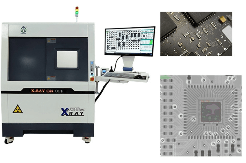
Printed circuit board (PCB) assembly demands rigorous quality control to ensure reliability in demanding applications. X-Ray inspection stands out as a non-destructive method to reveal hidden defects that optical or visual checks cannot detect. This technique penetrates multiple layers of copper, solder, and substrates to expose issues like solder voids, misalignments, cracks, delamination, and internal trace defects. For electric engineers working on high-density interconnects or ball grid array (BGA) components, understanding X-Ray inspection proves essential for failure prevention and process optimization. Factory-driven insights emphasize its role in meeting production yields and long-term performance standards. As PCB complexity increases with finer pitches and more layers, X-Ray becomes a cornerstone of quality assurance.
What Is PCB X-Ray Inspection and Why It Matters
PCB X-Ray inspection uses high-energy X-rays to generate images based on material density variations. Low-density areas, such as air pockets or gaps, appear darker, while denser materials like copper traces show brighter. Systems range from 2D transmission X-Ray for basic screening to 3D computed tomography (CT) or laminography for volumetric analysis. This method excels in inspecting bottom-terminated components, vias, and multilayer structures where surface inspection falls short. In modern electronics manufacturing, it directly impacts yield rates by identifying defects early, reducing rework costs, and enhancing reliability. Electric engineers rely on it to validate processes in high-volume production, especially for automotive, aerospace, and medical devices.
The relevance grows with shrinking component sizes and leadless packages. Traditional automated optical inspection (AOI) misses subsurface issues, but X-Ray provides comprehensive visibility. Factory protocols integrate it post-reflow soldering or after underfill application. Compliance with industry benchmarks ensures assemblies meet performance thresholds under thermal and mechanical stress. Ultimately, it safeguards against field failures that could arise from undetected anomalies.
Technical Principles of X-Ray Inspection
X-Ray inspection operates on the principle of differential absorption, where X-ray photons pass through the PCB but attenuate based on atomic number and thickness. A source emits a beam, which transmits through the sample onto a detector, forming a shadowgraph image. Tube voltage typically ranges from 30 to 160 kV, adjusted for penetration depth in thick boards or high-density areas. Magnification occurs via geometric setup, with oblique-angle views revealing hidden overlaps. Software enhances contrast, measures void percentages, and automates defect classification.
For multilayer PCBs, 2D X-Ray suffices for solder joint fillet checks but struggles with overlapping features. 3D techniques slice through the board virtually, eliminating superposition artifacts. Tilt and rotate capabilities expose pad-to-ball alignment precisely. Detector resolution, often sub-micron, captures fine cracks or trace interruptions. Engineers must calibrate systems for artifact minimization, such as beam hardening from varying materials. These principles enable accurate solder voids X-Ray detection and beyond.
Key Defects Detected by PCB X-Ray Inspection
Solder Voids X-Ray Detection
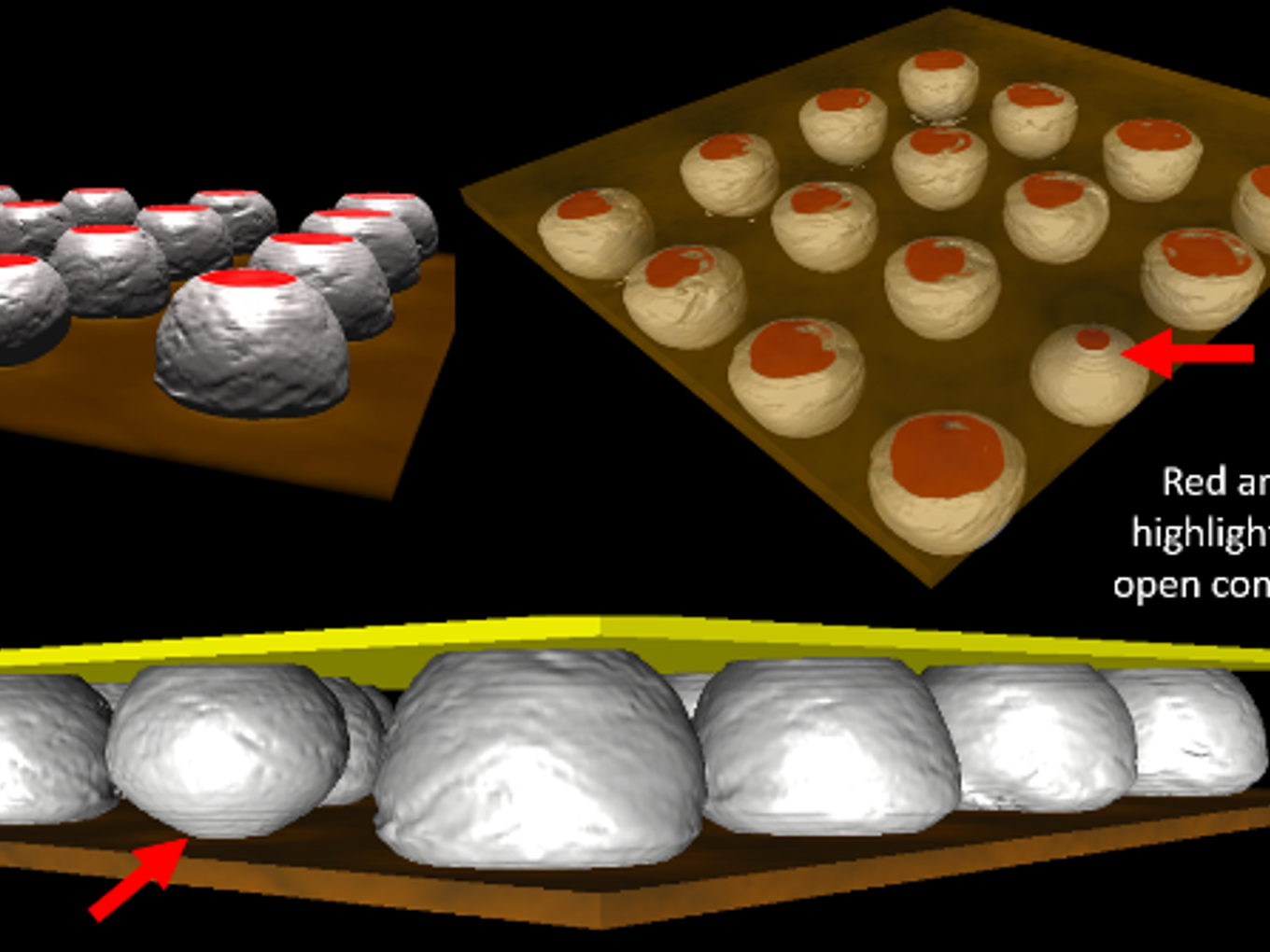
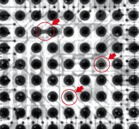
Solder voids form during reflow when flux volatiles or gases trap within the molten joint, creating low-density pockets. X-Ray images display these as dark spots against the uniform solder brightness. Critical in BGA, QFN, and QFP packages, voids compromise thermal conductivity and mechanical strength, accelerating fatigue under cycling. Detection involves measuring cumulative void area relative to joint size, with automated tools quantifying percentages across arrays. Factory scans post-reflow flag excessive voiding, prompting profile adjustments like nitrogen atmosphere use. Consistent monitoring prevents intermittents in high-reliability builds.
Component Misalignment X-Ray
Component misalignment X-Ray reveals offsets between pads and terminations, often from stencil printing errors or pick-and-place inaccuracies. In dense BGAs, shadows show ball offsets exceeding tolerances, risking open circuits or bridges. Oblique views confirm coplanarity and tilt, essential for fine-pitch devices. Misalignment stresses joints during thermal expansion, leading to cracks over time. Engineers analyze center-of-mass shifts to correlate with feeder vibrations or vision system drifts. Early detection via X-Ray maintains assembly integrity.
PCB Crack Detection
PCB crack detection targets fissures in vias, barrels, or surface traces invisible externally. X-Ray contrasts crack gaps as linear dark lines amid copper density. Barrel cracks from plating stress or drilling appear in plated through-holes (PTHs). Micro-cracks in inner layers signal laminate weaknesses or over-etching. High-resolution scans differentiate true cracks from artifacts like fiber weave. This inspection verifies board robustness before assembly.
Delamination X-Ray
Delamination X-Ray identifies layer separation due to moisture absorption, poor lamination, or CAF (conductive anodic filamentation). Gaps between cores show as uniform dark bands parallel to planes. Edge delamination risks during flexing, while internal ones short traces. Cross-section views via CT confirm extent and propagation. Process controls like bake-out prevent recurrence. Vital for HDI boards with thin dielectrics.
Internal Trace Defects X-Ray
Internal trace defects X-Ray uncovers opens, shorts, nicks, or mouse bites from inner-layer misalignment or etchant undercuts. High-contrast imaging differentiates traces from planes. Voids in dielectrics highlight plating voids or resin starvation. Multi-angle scans resolve overlaps in 12+ layer stacks. These defects cause signal integrity issues or power shorts. Routine bare-board X-Ray ensures layer registration.
Best Practices for PCB X-Ray Inspection
Select system parameters based on board thickness and material stackup. Higher kV penetrates thick FR-4 with copper planes, while lower settings sharpen thin flex circuits. Use geometric magnification for small features, balancing resolution and field of view. Automated programs set thresholds for void ratios, offsets, and crack widths per class definitions. Train operators on artifact recognition, like haloing from polychromatic beams.
Integrate X-Ray into the production flow: bare-board incoming, post-solder, and final AOI complement. Statistical process control tracks defect trends, linking to reflow profiles or paste rheology. For high-volume, oblique-angle scripting covers all joint quadrants. Reference IPC-A-610 for visual criteria analogs in X-Ray interpretation. Document anomalies with screenshots and measurements for root-cause analysis. These steps align factory outputs with reliability goals.
J-STD-001 outlines soldering process requirements that X-Ray verifies, ensuring material and method compliance. Calibrate detectors quarterly and maintain logbooks for traceability.
Troubleshooting Common X-Ray Inspection Challenges
Overlapping shadows plague 2D scans of dense areas; switch to laminography for pseudo-3D clarity. Beam hardening darkens thick sections unevenly, mitigated by filters or dual-energy sources. False positives from fiber weave texture require higher resolution or software normalization. For delamination mimics, correlate with C-scan ultrasound. Engineers troubleshoot by varying tilt angles and voltages iteratively. Case examples show void reductions after flux tweaks, confirmed via trend charts.
In one factory scenario, persistent BGA misalignment traced to nozzle wear, resolved post-X-Ray mapping. Crack detections prompted drill parameter audits, halving PTH failures. These insights drive continuous improvement.
Conclusion
PCB X-Ray inspection delivers unparalleled insight into hidden defects, from solder voids X-Ray detection to internal trace defects X-Ray analysis. Electric engineers benefit from its precision in validating complex assemblies against factory standards. Implementing best practices enhances yields and reliability. As designs evolve, advanced 3D systems will further refine detection. Prioritize it in quality protocols for robust electronics.
FAQs
Q1: How does solder voids X-Ray detection improve PCB reliability?
A1: Solder voids weaken joints by reducing cross-section and thermal paths, accelerating fatigue. X-Ray quantifies void percentages non-destructively, allowing process tweaks like optimized reflow ramps. Factory data shows early detection cuts field returns by identifying flux or paste issues. Align with standards for class-specific limits to ensure long-term performance.
Q2: What causes component misalignment X-Ray findings in SMT?
A2: Misalignment stems from pick-and-place offsets, stencil wear, or board warpage. X-Ray reveals pad-to-ball shifts precisely, preventing opens or stress concentrations. Troubleshoot via machine calibration and fiducial checks. Regular scans maintain tolerances under 50 microns for fine-pitch. Essential for HDI reliability.
Q3: Can X-Ray reliably perform PCB crack detection in vias?
A3: Yes, X-Ray contrasts crack gaps in PTH barrels or blind vias as dark lines. Differentiate from plating voids using multi-angle views. Combine with electrical testing for confirmation. Prevents intermittents in power delivery. Factory protocols flag them pre-assembly.
Q4: How does delamination X-Ray differ from visual checks?
A4: Visual methods miss internal delamination, but X-Ray shows layer gaps clearly. Caused by moisture or bond failures, it risks shorts. CT slices quantify depth. Bake and plasma clean prevent it. Critical for multilayer integrity.
References
IPC-A-610H — Acceptability of Electronic Assemblies. IPC, 2020
J-STD-001J — Requirements for Soldered Electrical and Electronic Assemblies. IPC, 2020
IPC-6012E — Qualification and Performance Specification for Rigid Printed Boards. IPC, 2017


