Introduction
Hand soldering for prototype PCB assembly stands as a fundamental skill for electrical engineers and designers aiming to bring electronic concepts to life. This technique enables rapid assembly and testing of designs without relying on automated processes, which are often impractical for small batch or one-off prototypes. Prototyping electronics with hand soldering offers flexibility, allowing immediate modifications and troubleshooting during the development phase. For engineers, mastering this craft ensures faster iterations and validates circuit functionality before moving to mass production. In this comprehensive guide, we explore the importance of hand soldering in fast PCB assembly, delve into essential techniques, and provide practical advice to achieve reliable results. Whether refining a new design or testing a concept, these insights aim to enhance your prototyping efficiency.
What Is Hand Soldering for Prototype PCB and Why It Matters
Hand soldering for prototype PCB refers to the manual process of joining electronic components to a printed circuit board using a soldering iron and solder material. Unlike automated methods such as wave or reflow soldering, this approach suits small scale projects where precision and adaptability are critical. It allows engineers to assemble and test designs quickly, often within hours, facilitating rapid feedback loops during development.
The significance of hand soldering in prototyping electronics lies in its accessibility and control. Engineers can place and connect components exactly as needed, make real time adjustments, and address issues on the spot. This method proves invaluable for validating circuit designs, ensuring functionality, and identifying potential flaws before committing to costly production runs. For fast PCB assembly in a lab or workshop setting, hand soldering remains a cornerstone of innovation and problem solving.
Technical Principles of Hand Soldering
Understanding the core principles of hand soldering ensures consistent and reliable connections. The process involves heating a soldering iron to a specific temperature, typically between 260 to 350 degrees Celsius, depending on the solder alloy and component sensitivity. This heat melts the solder, a metal alloy with a low melting point, allowing it to flow and bond the component lead to the PCB pad.
A key factor in successful soldering is thermal transfer. The soldering iron tip must maintain direct contact with both the component lead and the pad to heat them evenly. Solder then forms a metallurgical bond as it cools, creating a strong electrical and mechanical connection. Flux, a chemical agent often embedded in solder or applied separately, plays a vital role by removing oxides from surfaces, ensuring better wetting and adhesion.
Another critical principle is avoiding thermal damage. Excessive heat can degrade components or lift PCB traces. Adhering to guidelines such as those in IPC-A-610G, which outlines acceptability criteria for electronic assemblies, helps mitigate risks. Proper technique, including limiting contact time to a few seconds per joint, preserves the integrity of both components and the board.
Related Reading: Hand Soldering, PCB layout
Best Practices for Hand Soldering in Fast PCB Assembly
Achieving high quality results with hand soldering for prototype PCB requires adherence to proven practices. Below are actionable steps tailored for electrical engineers seeking efficiency and reliability during fast PCB assembly.
Preparation and Setup
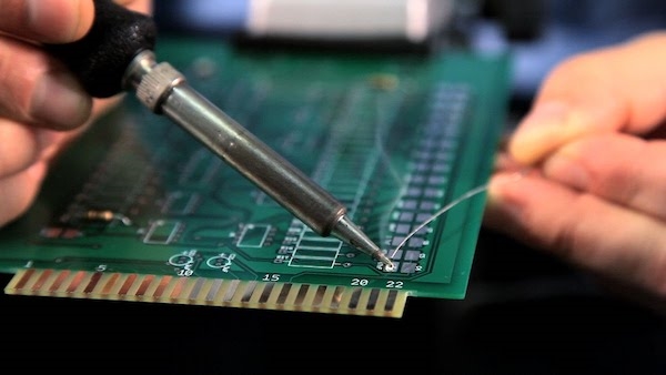
Start by organizing your workspace. Keep components, tools, and the PCB layout diagram within reach to minimize interruptions. Use a soldering iron with adjustable temperature control to match the requirements of your solder and components. A clean, tinned tip ensures optimal heat transfer, so wipe it on a damp sponge or use a brass wire cleaner before each session.
Select the appropriate solder, often a tin lead alloy with a 60/40 or 63/37 ratio for easier melting and flow, unless lead free is mandated. Ensure flux is available, either within the solder core or as a separate application, to improve joint quality. Secure the PCB in a holder or vise to prevent movement during soldering.
Soldering Technique
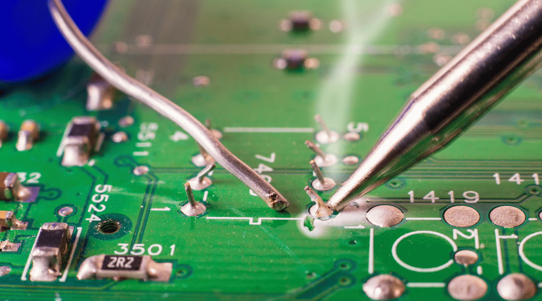
Begin with smaller components like resistors and capacitors before moving to larger ones. This sequence prevents obstruction and simplifies positioning. Place the soldering iron tip at the junction of the component lead and PCB pad, heating both for about two seconds. Introduce solder to the joint, allowing it to flow naturally around the lead and pad, forming a shiny, conical shape.
Avoid applying excessive solder, which can create bridges between pads, leading to short circuits. If a joint appears dull or grainy, indicating a cold solder joint, reheat it briefly and add a small amount of fresh solder. Limit heat exposure to prevent damage, aligning with standards like IPC-A-610G for acceptable soldering outcomes.
Post Soldering Inspection and Cleanup
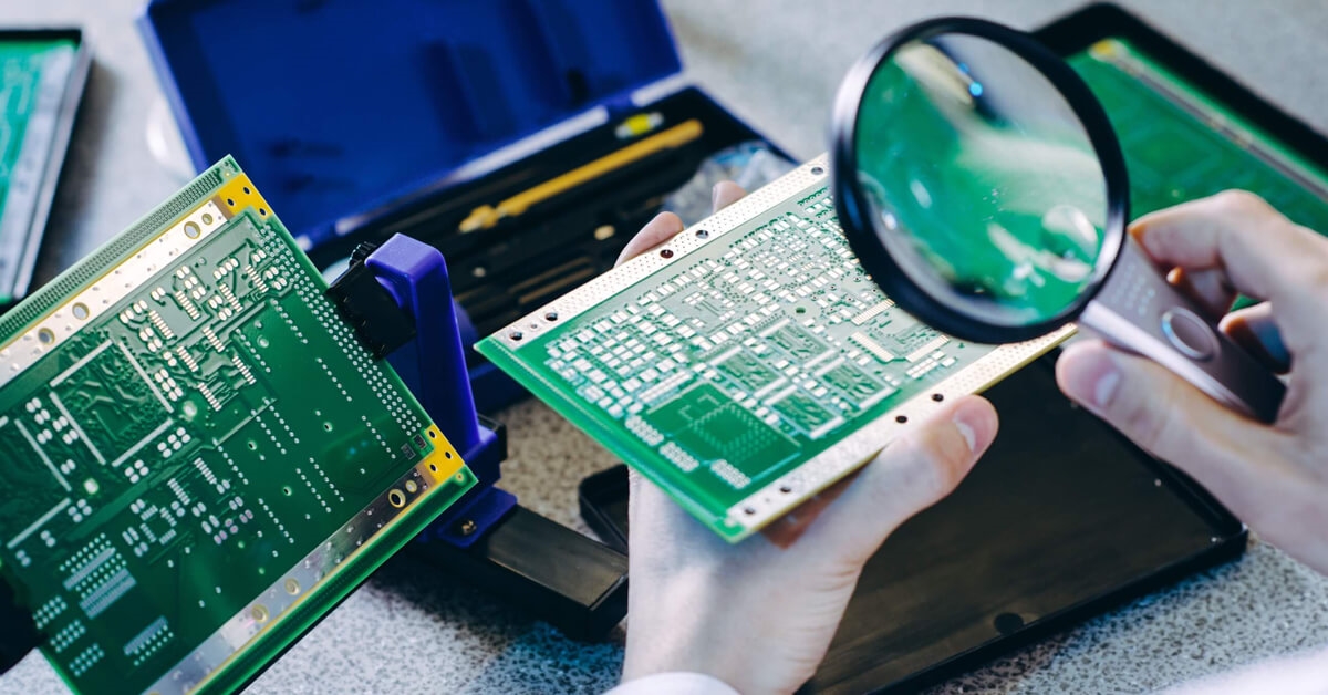
After soldering, inspect each joint visually for consistency and shape. A magnifying glass or microscope can reveal defects like insufficient solder or cracks. Test the circuit for continuity using a multimeter to confirm electrical connections. Remove excess flux residue with isopropyl alcohol and a brush, as buildup can cause corrosion over time.
Trim component leads close to the joint using flush cutters, ensuring no sharp edges remain. Document any issues encountered during assembly to refine future prototypes. This systematic approach supports fast PCB assembly while maintaining quality.
Avoiding Common Pitfalls
Several errors can compromise hand soldering quality. Overheating is a frequent issue, so monitor temperature settings and soldering duration. Cold joints, caused by insufficient heat or movement during cooling, lead to unreliable connections. Ensure stable contact and adequate heat before applying solder.
Solder bridges occur when excess solder connects adjacent pads. Use a desoldering braid or sucker to remove unwanted solder if this happens. Finally, avoid poor component placement by double checking orientations, especially for polarized components like diodes and capacitors, to prevent circuit failure.
Troubleshooting Challenges in Prototyping Electronics with Hand Soldering
During prototyping electronics with hand soldering, engineers often encounter specific challenges. Addressing these promptly ensures project timelines remain on track. One common issue is lifted pads, where excessive heat or mechanical stress detaches the copper trace from the PCB. To mitigate this, use minimal heat and avoid pulling on component leads during soldering.
Another challenge is soldering surface mount components, which are smaller and more delicate than through hole parts. Use a fine tip soldering iron and apply solder sparingly to prevent bridging. Tweezers can assist in positioning components accurately before securing them.
If a joint fails to conduct properly, verify the connection with a multimeter. Poor conductivity often stems from insufficient solder or oxide buildup, resolved by cleaning the surfaces with flux and resoldering. For complex designs, consider creating a soldering sequence plan to manage densely populated boards without thermal interference between adjacent components.
Related Reading: The Do's and Don'ts of Hand Soldering: Avoiding Common Pitfalls for Optimal Results
Conclusion
Hand soldering for prototype PCB assembly empowers electrical engineers to transform ideas into functional designs with speed and precision. By mastering the technical principles and adhering to best practices, professionals can achieve reliable connections essential for fast PCB assembly. Proper preparation, technique, and troubleshooting address common challenges in prototyping electronics with hand soldering, ensuring efficient iterations. As a cornerstone of electronic development, this skill enables rapid testing and refinement, paving the way for successful product outcomes. Embrace these strategies to streamline your prototyping process and elevate design quality.
FAQs
Q1: How does hand soldering for prototype PCB differ from automated assembly?
A1: Hand soldering for prototype PCB involves manually joining components using a soldering iron, ideal for small scale testing and quick modifications. Automated assembly, guided by standards like IPC-A-610G, uses machines for high volume production with consistent precision. Hand soldering offers flexibility for engineers to adjust designs on the fly, while automation prioritizes speed and uniformity for finalized products.
Q2: What tools are essential for prototyping electronics with hand soldering?
A2: For prototyping electronics with hand soldering, a temperature controlled soldering iron is critical for precision. Additional tools include solder wire, flux, tweezers for component placement, a desoldering braid for corrections, and a multimeter for testing. A stable holder for the PCB prevents movement. These tools ensure efficient assembly and reliable connections during prototype development.
Q3: How can I achieve fast PCB assembly with hand soldering without compromising quality?
A3: To achieve fast PCB assembly with hand soldering, organize components and tools beforehand to minimize delays. Follow a logical soldering sequence, starting with smaller parts. Use appropriate heat settings to avoid damage, adhering to guidelines like IPC-A-610G. Inspect joints visually and test electrically after soldering. This structured approach maintains quality while speeding up the process.
Q4: What are common defects to watch for in hand soldering prototype PCBs?
A4: In hand soldering for prototype PCB, watch for cold joints, appearing dull due to insufficient heat, and solder bridges causing shorts. Lifted pads from overheating and poor wetting from inadequate flux are also issues. Inspect joints per IPC-A-610G standards using magnification. Correct defects by reheating or removing excess solder to ensure reliable connections.
References
IPC-A-610G — Acceptability of Electronic Assemblies. IPC, 2017.
IPC-A-600K — Acceptability of Printed Boards. IPC, 2020.


