Introduction
High Density Interconnect (HDI) technology has become a cornerstone in modern electronics, enabling compact and high-performance printed circuit boards (PCBs). As devices shrink in size while increasing in functionality, HDI assembly demands precise design practices to ensure manufacturability. Design for Manufacturability (DFM) plays a critical role in bridging the gap between innovative designs and reliable production. This article explores key DFM guidelines tailored for HDI assembly, focusing on microvias, trace width, annular rings, and PCB layout strategies. By adhering to industry standards and best practices, engineers can minimize manufacturing defects, reduce costs, and enhance product reliability. Whether you are designing for consumer electronics or industrial applications, understanding these principles is essential for successful HDI implementation.
What Is HDI Assembly and Why DFM Matters
HDI assembly refers to the process of building PCBs with densely packed components, fine traces, and advanced interconnection techniques like microvias. These boards often feature multiple layers with reduced spacing, catering to miniaturized electronics such as smartphones and medical devices. The complexity of HDI designs introduces unique manufacturing challenges, including alignment precision and thermal stress management.
DFM in HDI assembly focuses on creating designs that align with fabrication and assembly capabilities. Without proper DFM, issues like misaligned microvias, insufficient annular rings, or improper trace width can lead to failures during production. Implementing DFM rules ensures higher yields, reduces rework, and accelerates time to market. For electrical engineers, integrating manufacturability into the design phase is not just a best practice but a necessity for achieving consistent quality in high density layouts.
Technical Principles of HDI DFM
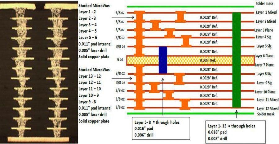
Understanding Microvias in HDI Design
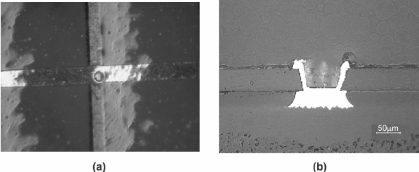
Microvias are small diameter vias, typically less than 0.15 mm, used to connect layers in HDI PCBs. They enable higher routing density by reducing the space needed for interconnections. However, their small size makes them prone to manufacturing defects like incomplete plating or structural weaknesses. Engineers must consider aspect ratio, the ratio of via depth to diameter, to ensure reliable drilling and plating. Following industry guidelines, such as those in IPC-2226, helps define acceptable parameters for microvia design and placement.
Trace Width and Spacing Constraints
Trace width and spacing are critical in HDI layouts due to the limited real estate on the board. Narrow traces are necessary for fitting more connections, but they must carry sufficient current without overheating. Spacing between traces must prevent crosstalk and maintain signal integrity. Adhering to standards like IPC-2221 ensures that trace width and spacing meet electrical and thermal requirements. Balancing these factors during the design phase directly impacts manufacturability and performance.
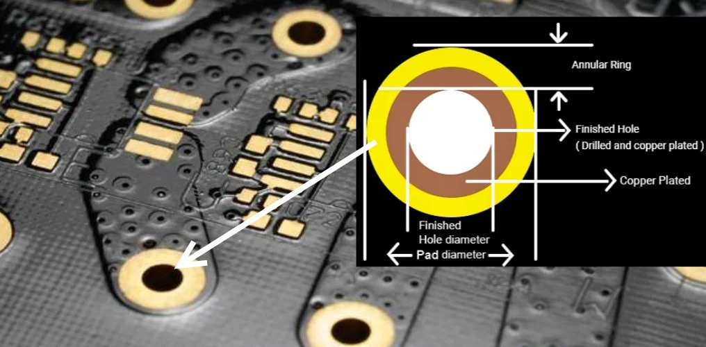
Annular Rings and Their Role
Annular rings are the copper pads surrounding vias or through holes, providing structural support and electrical connectivity. In HDI designs, where space is constrained, maintaining adequate annular ring size is challenging yet vital. Insufficient rings can lead to weak connections or drilling misalignments during fabrication. Guidelines from IPC-A-600K emphasize the minimum acceptable annular ring dimensions to avoid defects. Proper design of these rings enhances the board's mechanical strength and assembly reliability.
Practical Solutions and Best Practices for HDI DFM
Optimizing Microvia Placement and Stackup
To improve manufacturability, position microvias strategically within the PCB layout. Avoid stacking multiple microvias directly on top of each other unless supported by advanced fabrication processes, as this can lead to reliability issues. Instead, stagger microvias across layers to distribute stress. Additionally, consult IPC-2226 for stackup design rules that balance layer count with microvia usage. A well planned stackup minimizes drilling complexities and enhances signal integrity during assembly.
Defining Trace Width and Spacing Parameters
When determining trace width, consider both current carrying capacity and thermal dissipation needs. Use established standards like IPC-2221 to calculate appropriate widths based on expected current and temperature rise. For spacing, maintain clearance to prevent electrical interference, especially in high speed designs. Collaborate with fabricators early to align design rules with their capabilities. This proactive approach reduces the risk of manufacturing bottlenecks and ensures consistent trace quality.
Ensuring Adequate Annular Rings
Design annular rings with sufficient width to support drilling tolerances and maintain connection integrity. Reference IPC-A-600K for minimum ring sizes based on via type and board class. Account for potential registration errors during fabrication by providing extra margin where possible. Regularly review design files against these standards to catch issues before production. Strong annular rings are fundamental to preventing via failures and ensuring long term reliability in HDI assemblies.
Streamlining PCB Layout for Assembly
A manufacturable PCB layout prioritizes component placement and routing efficiency. Group components logically to minimize trace lengths and reduce signal delays. Keep high speed signals away from noisy areas to preserve integrity. Incorporate test points for easier debugging during assembly and quality control. Following DFM guidelines, such as those outlined in IPC-7351, helps create layouts that simplify soldering and inspection processes. An optimized layout directly translates to fewer assembly errors and smoother production runs.
Thermal Management in HDI Designs
HDI boards often face thermal challenges due to their compact nature and high component density. Integrate thermal vias and heat sinks where necessary to dissipate heat effectively. Ensure that trace widths near power components are adequate to handle thermal loads without degradation. Refer to IPC-2152 for guidance on designing for thermal performance. Proper thermal planning during the design stage prevents overheating issues that could compromise assembly quality and product lifespan.
Troubleshooting Common HDI DFM Issues
As an assembly engineer, I have encountered recurring challenges in HDI projects that stem from overlooking DFM principles. One frequent issue is microvia failure due to improper aspect ratios or plating defects. To address this, always validate microvia designs against IPC-2226 standards and conduct thorough design reviews. Another common problem is insufficient annular rings leading to broken connections after soldering. Cross checking ring dimensions with IPC-A-600K during the layout phase can prevent such defects.
Trace width errors also pose significant risks, especially when designs push manufacturing limits without fabricator input. I recommend establishing clear communication with production teams to align on feasible trace and spacing rules. Lastly, poor PCB layout often complicates assembly, causing misalignments or soldering issues. Prioritizing component grouping and routing clarity, as per IPC-7351, resolves many of these bottlenecks. Drawing from experience, early collaboration and adherence to standards are the most effective ways to troubleshoot and mitigate HDI assembly challenges.
Conclusion
Design for Manufacturability is a fundamental aspect of successful HDI assembly, ensuring that complex designs translate into reliable, high quality products. By focusing on critical elements like microvias, trace width, annular rings, and PCB layout, engineers can address potential manufacturing hurdles upfront. Adhering to established industry standards, such as those from IPC, provides a solid framework for creating designs that align with fabrication and assembly capabilities. Implementing the best practices discussed, from optimizing stackups to enhancing thermal management, empowers teams to achieve higher yields and consistent performance. For electrical engineers, mastering DFM in HDI assembly is not only about meeting technical requirements but also about driving efficiency and innovation in every project.
FAQs
QX: How do microvias impact HDI assembly manufacturability?
AX: Microvias are essential for high density routing in HDI PCBs but pose manufacturability challenges due to their small size. Issues like incomplete plating or high aspect ratios can lead to failures. Following standards like IPC-2226 ensures proper design and placement, reducing defects. Early collaboration with fabricators also helps align microvia specifications with production capabilities for reliable assembly outcomes.
QX: What are the key DFM rules for trace width in HDI designs?
AX: Trace width in HDI designs must balance current capacity and thermal performance while fitting within tight spaces. IPC-2221 provides guidelines for calculating appropriate widths based on electrical needs. Maintaining adequate spacing prevents interference and ensures signal integrity. Consulting fabricators on minimum achievable widths is crucial to avoid manufacturing issues and ensure consistent quality.
QX: Why are annular rings critical for PCB layout in HDI boards?
AX: Annular rings provide structural support and electrical connectivity around vias in HDI PCBs. Inadequate ring size can cause weak connections or drilling errors, impacting reliability. IPC-A-600K outlines minimum dimensions to prevent such defects. Proper annular ring design within the PCB layout enhances mechanical strength and ensures robust assembly under tight spacing constraints.
QX: How can PCB layout optimize HDI assembly processes?
AX: An optimized PCB layout in HDI assembly minimizes trace lengths, groups components logically, and incorporates test points for easier debugging. Following IPC-7351 guidelines ensures efficient routing and soldering. Keeping high speed signals isolated from noise sources preserves performance. A well structured layout reduces assembly errors, streamlines production, and improves overall manufacturability of the board.
References
IPC-2226 - Design Standard for High Density Interconnect (HDI) Printed Boards. IPC, 2003.
IPC-2221 - Generic Standard on Printed Board Design. IPC, 2021.
IPC-A-600K - Acceptability of Printed Boards. IPC, 2020.
IPC-7351 - Generic Requirements for Surface Mount Design and Land Pattern Standard. IPC, 2010.
IPC-2152 - Standard for Determining Current Carrying Capacity in Printed Board Design. IPC, 2009.


