Introduction
High-Density Interconnect (HDI) technology plays a critical role in modern electronics by enabling compact, high-performance printed circuit boards (PCBs). As devices shrink in size while demanding greater functionality, HDI assembly has become essential for achieving intricate designs with improved electrical performance and effective thermal management. This article explores HDI stack-up structures and materials, focusing on layer count, material selection, and their impact on PCB design. By understanding these elements, electrical engineers can optimize designs for reliability and efficiency in demanding applications. The following sections provide a detailed look into the principles of HDI stack-ups, material choices, and best practices for balancing electrical and thermal needs in PCB assembly.
What Is HDI Assembly and Why It Matters
HDI assembly refers to the process of constructing PCBs with high-density interconnects, characterized by finer lines, smaller vias, and denser component placement compared to traditional boards. This technology is vital for applications in smartphones, medical devices, and aerospace systems where space is limited and performance is paramount. HDI stack-ups often incorporate microvias, blind vias, and buried vias to achieve compact routing and minimize signal loss. The significance of HDI lies in its ability to support high-speed signals and manage heat dissipation in tightly packed designs. For engineers, mastering HDI assembly ensures that designs meet stringent performance criteria while maintaining manufacturability and reliability under challenging operating conditions.
Technical Principles of HDI Stack-Up Structures
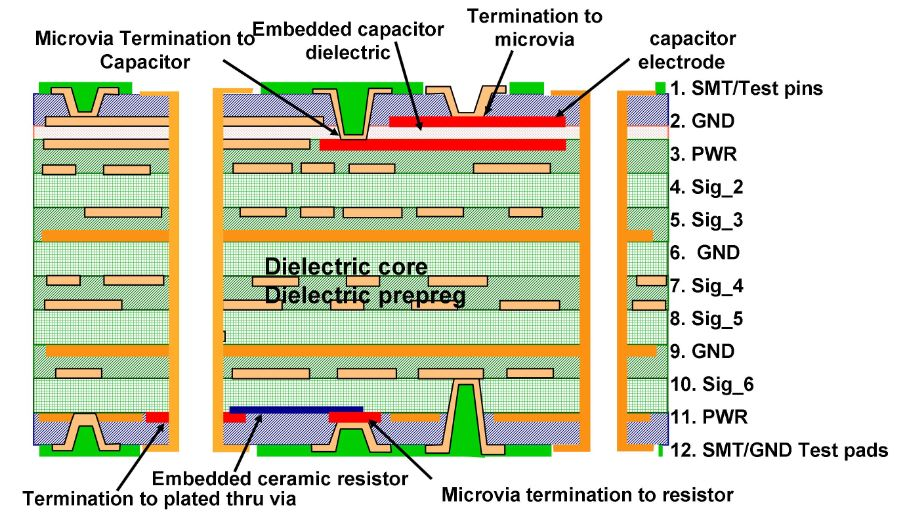
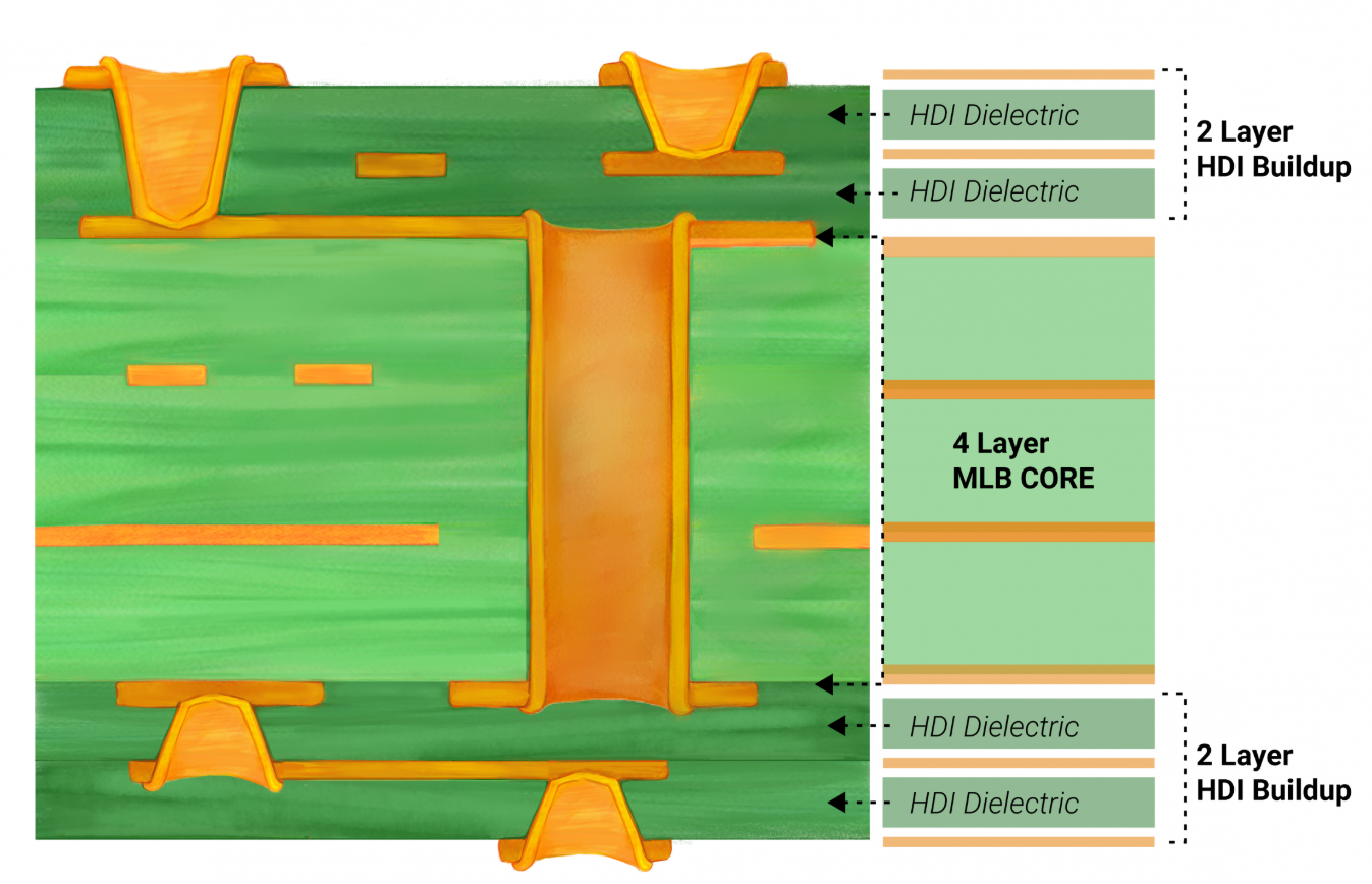
HDI stack-up structures define the arrangement of conductive and insulating layers in a PCB, directly influencing electrical performance and thermal management. These structures typically involve multiple layers, often exceeding six, with intricate via configurations to connect components across layers. Microvias, which are smaller than traditional through-hole vias, are a hallmark of HDI designs, allowing for higher routing density. Blind vias connect an outer layer to an inner layer without passing through the entire board, while buried vias link internal layers, saving surface space.
Layer count in HDI designs varies based on complexity, with common configurations ranging from 1-N-1 to 2-N-2, where "N" represents core layers, and the numbers indicate build-up layers on each side. A higher layer count enables more routing options but increases fabrication challenges and thermal concerns. The stack-up must balance signal integrity by minimizing crosstalk and impedance mismatches, often achieved through controlled dielectric thickness and proper ground plane placement. Standards such as IPC-2226, which provides guidelines for HDI design, emphasize the importance of via structure and layer symmetry to prevent warpage and ensure reliability during assembly.
Thermal management is another critical aspect influenced by stack-up design. Heat generated by high-performance components must be dissipated efficiently to prevent failures. Incorporating thermal vias and ensuring adequate copper thickness in power planes can enhance heat transfer. Engineers must also consider the stack-up's impact on signal paths, as longer traces or improper via placement can degrade electrical performance. By adhering to established guidelines, such as those in IPC-2226, designers can create HDI stack-ups that meet both electrical and thermal demands.
Material Selection for HDI PCBs
Material selection is a cornerstone of HDI assembly, affecting both electrical performance and thermal management. The primary materials in HDI PCB design include the dielectric substrate, copper foils, and prepreg layers used for bonding. Dielectric materials must exhibit low loss tangent and stable dielectric constant to support high-speed signals, especially in applications exceeding 1 GHz. High glass transition temperature (Tg) materials are often preferred for HDI boards to withstand multiple reflow cycles during assembly without degrading.
Common dielectric materials for HDI designs are categorized by their thermal and electrical properties. Materials with higher Tg values, typically above 170 degrees Celsius, offer better stability under heat stress, which is crucial for multilayer boards with dense component layouts. Low-loss dielectrics are selected for high-frequency applications to reduce signal attenuation. Copper thickness, often specified in ounces per square foot, must be chosen based on current-carrying requirements and thermal dissipation needs. Thinner copper layers save space in HDI designs but may limit heat transfer, necessitating a careful balance.
Prepreg materials, used to bond layers in multilayer HDI stack-ups, must match the core dielectric properties to avoid mismatches in thermal expansion. Standards such as IPC-4101, which outline specifications for base materials, provide guidance on selecting laminates and prepregs for consistent performance. Thermal conductivity of materials also plays a role, as poor heat dissipation can lead to hotspots, impacting component lifespan. Engineers must evaluate material properties against design goals to ensure reliability, particularly in environments with fluctuating temperatures or high power demands.
Impact on Electrical Performance
Electrical performance in HDI assembly is heavily influenced by stack-up structure and material selection. Signal integrity, a primary concern, depends on controlled impedance, which requires precise dielectric thickness and consistent material properties. In HDI designs, shorter signal paths enabled by microvias reduce delay and reflection, enhancing performance at high frequencies. However, improper stack-up design, such as uneven layer distribution, can introduce crosstalk or electromagnetic interference.
Ground and power planes are critical for maintaining stable voltage levels and minimizing noise. Placing these planes adjacent to signal layers in the stack-up provides shielding and reduces loop inductance. Layer count affects routing flexibility; more layers allow for dedicated planes but increase complexity. Materials with low dielectric loss are essential for high-speed signals to prevent energy dissipation. Adhering to guidelines in IPC-2221, which covers design standards for PCBs, helps ensure that electrical performance meets application requirements through proper stack-up planning and material choices.
Strategies for Thermal Management in HDI Designs
Thermal management is a significant challenge in HDI assembly due to the high density of components and limited space for heat dissipation. Effective strategies begin with stack-up design, where thermal vias are strategically placed to transfer heat from critical areas to outer layers or heat sinks. These vias, often filled with conductive materials, create direct paths for heat flow, reducing temperature buildup in inner layers.
Material selection also impacts thermal performance. Substrates with higher thermal conductivity can distribute heat more evenly across the board, preventing localized hotspots. Copper planes, when designed with sufficient thickness, act as thermal spreaders, especially in power-intensive applications. Engineers must also consider the coefficient of thermal expansion (CTE) of materials to avoid stress during temperature changes, which could lead to delamination or cracking. Guidelines from IPC-6012E, which addresses performance specifications for rigid boards, highlight the need for thermal reliability in multilayer PCB designs.
Via-in-pad structures offer another solution by providing direct thermal and electrical connections under components. This approach requires careful fabrication to ensure void-free filling, maintaining both thermal and structural integrity. Balancing layer count is equally important, as excessive layers can trap heat, while insufficient layers limit routing and thermal paths. By integrating these strategies, engineers can mitigate thermal risks and extend the operational life of HDI assemblies.
Best Practices for HDI Stack-Up Design and Assembly
Creating an effective HDI stack-up requires a systematic approach to layer configuration and material selection. Start by defining the layer count based on routing needs and component density, ensuring symmetry to minimize warpage risks. Use simulation tools to verify impedance control and signal integrity before finalizing the design. Incorporate dedicated ground and power planes to stabilize electrical performance, positioning them close to signal layers for optimal shielding.
Select materials that align with both electrical and thermal requirements. Prioritize dielectrics with low loss for high-speed signals and high Tg for thermal stability. Ensure compatibility between core and prepreg materials to prevent issues during lamination. Thermal vias and via-in-pad structures should be planned early to address heat dissipation, particularly under high-power components. Follow standards like IPC-2226 for via design and stack-up guidelines to maintain manufacturability.
During assembly, verify that fabrication processes support the chosen stack-up and materials. Communicate design intent clearly to ensure microvias and buried vias are executed without defects. Test prototypes under operating conditions to validate electrical performance and thermal behavior, adjusting the design if necessary. These practices help achieve reliable HDI assemblies that perform consistently in demanding environments.
Conclusion
HDI assembly is a complex yet essential process for modern PCB design, requiring careful consideration of stack-up structures and materials. Layer count, via configurations, and material properties directly influence electrical performance and thermal management, impacting the reliability of compact, high-density electronics. By adhering to industry standards and implementing best practices, engineers can create HDI designs that balance performance with manufacturability. Understanding these principles ensures that designs meet the rigorous demands of advanced applications, paving the way for innovation in electronics.
FAQs
Q1: What factors influence HDI stack-up design for electrical performance?
A1: HDI stack-up design impacts electrical performance through layer count, via placement, and dielectric properties. Controlled impedance, achieved with precise material selection and layer arrangement, minimizes signal loss. Ground planes reduce noise, while microvias shorten signal paths. Following standards like IPC-2221 ensures reliable performance in high-speed applications.
Q2: How does material selection affect thermal management in HDI PCBs?
A2: Material selection is critical for thermal management in HDI PCBs. High Tg dielectrics withstand heat during assembly, while substrates with better thermal conductivity distribute heat evenly. Copper thickness aids dissipation. Matching CTE values prevents stress, ensuring reliability under thermal cycles as per IPC-6012E guidelines.
Q3: Why is layer count important in HDI PCB design?
A3: Layer count in HDI PCB design determines routing capacity and complexity. More layers offer flexibility for dense designs but increase thermal challenges. Symmetry in stack-ups prevents warpage. Balancing layer count with application needs ensures optimal electrical performance and manufacturability, guided by standards like IPC-2226.
Q4: What are key considerations for via structures in HDI stack-ups?
A4: Via structures in HDI stack-ups, such as microvias and blind vias, must optimize space and signal paths. Thermal vias enhance heat dissipation, while via-in-pad designs support compact layouts. Proper fabrication, as outlined in IPC-2226, ensures reliability and prevents defects during assembly processes.
References
IPC-2226 — Design Standard for High Density Interconnect (HDI) Printed Boards. IPC, 2003.
IPC-2221 — Generic Standard on Printed Board Design. IPC, 2021.
IPC-4101 — Specification for Base Materials for Rigid and Multilayer Printed Boards. IPC, 2021.
IPC-6012E — Qualification and Performance Specification for Rigid Printed Boards. IPC, 2020.


