Introduction
Automated Optical Inspection (AOI) equipment plays a critical role in modern PCB manufacturing by identifying defects at high speeds and with consistent accuracy. As production volumes increase and component densities rise, manual inspection becomes impractical, leading to higher error rates and yield losses. AOI systems use advanced imaging and algorithms to scan assembled boards, detecting issues that could compromise reliability or functionality. This visual guide explores how AOI equipment detects common PCB defects, focusing on key areas like solder joints, component placement, and polarity. Engineers benefit from understanding these mechanisms to optimize inspection processes and align with quality standards. By integrating AOI effectively, factories reduce rework and enhance overall process control.
What Is AOI Equipment and Why It Matters in PCB Quality Control
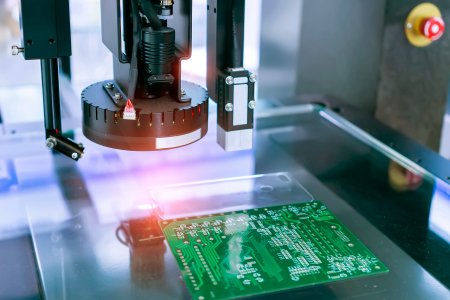
AOI equipment refers to automated systems that employ high-resolution cameras, precise lighting, and sophisticated software to visually inspect PCBs during manufacturing. These systems typically operate post-surface mount technology (SMT) placement or after reflow soldering, comparing captured images against reference data from CAD files or golden samples. Unlike manual visual checks, AOI provides objective, repeatable results, minimizing human fatigue and variability. In high-mix, high-volume environments, AOI equipment catches AOI equipment PCB defects early, preventing costly downstream failures in functional testing or field deployment. Its importance grows with miniaturization trends, where defects like micro-bridges or subtle misalignments evade naked-eye detection. Factory-driven insights emphasize AOI's alignment with standards such as IPC-A-610, ensuring assemblies meet class 2 or class 3 criteria for commercial or high-reliability applications.
The relevance of AOI extends to yield improvement and cost savings. Defects undetected at this stage propagate to in-circuit testing (ICT) or final assembly, amplifying expenses through scrap or repair. AOI equipment supports just-in-time manufacturing by flagging issues in real-time, allowing immediate process adjustments like feeder calibration or stencil cleaning. For electric engineers, mastering AOI integration means balancing sensitivity settings to avoid false calls while capturing all critical AOI equipment defect types. Ultimately, AOI bridges the gap between automated assembly and quality assurance, upholding factory standards in competitive production lines.
Core Technologies in AOI Equipment for Defect Detection
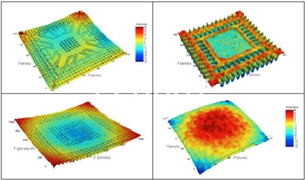
AOI equipment relies on optical imaging principles, including multiple camera angles and structured illumination to capture 2D or 3D profiles of the PCB surface. In 2D systems, grayscale or color images undergo pattern matching and edge detection algorithms to identify anomalies against programmed fiducials and component outlines. 3D AOI adds height measurement via laser triangulation or moiré projection, enabling volumetric analysis crucial for solder joint quality. Software processes these images in milliseconds per field of view, classifying defects based on predefined thresholds for position, size, and shape. Lighting configurations, such as coaxial, oblique, or multi-spectrum, enhance contrast for reflective solder or matte components. These technologies collectively enable comprehensive coverage of AOI equipment PCB defects across bare boards, pre-reflow, and post-reflow stages.
Factory implementations often program AOI with tolerance bands derived from design rules and process capabilities. Algorithms employ machine learning in advanced models to adapt to variations like shadow artifacts or board warpage. Detection accuracy hinges on calibration, where reference boards establish baselines for nominal features. Engineers adjust parameters like pixel resolution, typically 10-20 microns, to match component pitch down to 0.3mm QFN packages. This technical foundation ensures AOI equipment reliably flags deviations, supporting data-driven root cause analysis in quality control loops.
How AOI Equipment Performs Solder Joint Inspection
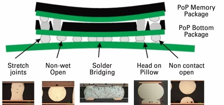
AOI equipment solder joint inspection scrutinizes fillet formation, wetting, and joint symmetry using shape recognition and height profiling. Post-reflow, cameras capture side profiles to verify heel-toe fillet curves, which indicate proper solder flow per IPC-A-610 guidelines. Bridges appear as unintended conductive paths between adjacent pads, detected by excess material bridging gaps smaller than specified isolation distances. Insufficient solder manifests as concave or absent fillets, while excess solder forms peaks or balls, both triggering alerts via volume measurements in 3D systems. Tombstoning, where components lift due to uneven reflow, shows height disparities exceeding tolerances. These checks prevent intermittent opens or shorts that plague high-density boards.
In practice, AOI algorithms segment joint areas using edge detection, then compute metrics like meniscus angle and standoff height. Oblique lighting reveals surface cracks or dewetting, where solder fails to adhere uniformly. Multi-angle imaging mitigates specular reflections from shiny joints, ensuring consistent detection. Engineers fine-tune thresholds based on alloy type and pad finish, such as ENIG or HASL, to minimize escapes. By quantifying joint quality, AOI equipment solder joint inspection integrates seamlessly with statistical process control, correlating defects to reflow profiles or paste volume.
Detecting Component Placement Errors with AOI Equipment
AOI equipment component placement verifies XY positioning, rotation, and presence by overlaying captured images on reference templates. Misalignment, or offset, occurs when centers deviate beyond process windows, often from pick-and-place inaccuracies, flagged by bounding box discrepancies. Skewed components, rotated beyond 5-10 degrees depending on package type, disrupt pin-to-pad registration and are quantified via principal axis analysis. Missing parts create voids in expected locations, while flipped or wrong-value components mismatch size, shape, or marking patterns. 3D profiling confirms coplanarity, essential for BGA balls or tall passives. These AOI equipment component placement checks maintain assembly integrity before reflow solidification.
Software employs template matching with sub-pixel accuracy to tolerate minor feeder vibrations. Fiducial marks on the PCB provide global alignment references, compensating for conveyor-induced shifts. Detection speed scales with resolution, inspecting thousands of components per minute. Factory best practices include verifying placement post-SMT but pre-reflow to enable rework without thermal stress. For electric engineers, analyzing AOI placement data reveals systemic issues like nozzle wear, optimizing machine nozzels and vision systems upstream.
AOI Equipment Polarity Checks and Orientation Verification
AOI equipment polarity check relies on visual feature recognition to ensure correct orientation of diodes, LEDs, electrolytic capacitors, and ICs. Polarity markings, such as stripes, beveled edges, or silkscreen indicators, are compared against library images for match verification. Inverted components show reversed patterns, triggering immediate flags during scan. For symmetric packages with internal asymmetry, like tantalum caps, shape profiling distinguishes cathode-anode features. Multi-spectral imaging aids faint markings under solder mask. This prevents functional failures from reverse biasing or incorrect pinouts in downstream operation.
Algorithms use optical character recognition (OCR) for alphanumeric codes alongside geometric checks, achieving near-100% accuracy on standard parts. Programming includes golden sample training to capture real-world variations in printing quality. Post-placement timing catches errors before reflow locks them in place. Per J-STD-001 requirements, proper polarity ensures solder joint reliability under thermal cycling. Engineers leverage polarity defect trends to audit programming data against BOM, closing the loop on design-to-assembly fidelity.
Other AOI Equipment Defect Types in PCB Inspection
Beyond core areas, AOI equipment defect types encompass bare board issues like conductor opens, shorts, and surface contaminants. Scratches or stains on solder masks alter reflectance, detected via intensity thresholding. Warpage exceeding 0.75% of board dimension distorts fiducials, measured in 3D modes to predict assembly challenges. Wrong parts, identified by dimension mismatches, protect against value errors invisible to placement machines. Pin shorts or lifted leads complete the spectrum, with reporting tied to zone coordinates for traceability.
Comprehensive programming covers these via layered inspections, from bare PCB to fully loaded. Integration with SPI (solder paste inspection) upstream enhances overall defect capture. Data analytics from AOI logs Pareto charts for process hotspots, aligning with ISO 9001 quality systems.
Best Practices for AOI Implementation and Troubleshooting
Select AOI equipment based on board complexity, favoring 3D for fine-pitch BGAs and high-lead-count devices. Program using CAD import and golden board verification to establish baselines, iterating thresholds with process engineers. Regular calibration with standards like IPC-A-600 maintains accuracy amid environmental drifts. Minimize false calls by optimizing lighting for matte finishes and programming tolerances to CpK >1.33.
Troubleshooting involves reviewing false positives from glue dots or flux residue, adjustable via region-of-interest exclusions. Yield correlation studies link AOI escapes to downstream ICT fails, refining algorithms. Operator training on report interpretation ensures swift rework. These practices elevate AOI from inspection tool to process sentinel.
Conclusion
AOI equipment transforms PCB quality control by visually detecting solder joint anomalies, placement errors, polarity issues, and more with precision unattainable manually. Factory engineers gain actionable insights from its data-rich outputs, driving continuous improvement. Adhering to standards like IPC-A-610 and J-STD-001 ensures compliance across production classes. Integrating AOI strategically boosts yields, cuts costs, and safeguards reliability in demanding applications. As PCB densities evolve, AOI remains indispensable for scalable, defect-free manufacturing.
FAQs
Q1: What are the main AOI equipment PCB defects it can detect?
A1: AOI equipment PCB defects include solder bridges, missing components, misalignment, and polarity errors. It scans using cameras and algorithms to compare against references, flagging issues post-placement or reflow. This factory-aligned approach per IPC standards prevents yield loss without manual intervention. Integration yields high throughput for electric engineers optimizing lines.
Q2: How does AOI equipment solder joint inspection work?
A2: AOI equipment solder joint inspection analyzes fillet shape, volume, and wetting via 2D/3D imaging. Bridges show as excess connections, insufficient joints lack proper heels, detected against tolerance bands. Lighting enhances contrast for cracks or voids. Engineers adjust for pad types, ensuring J-STD-001 compliance in reflow processes.
Q3: What role does AOI equipment component placement play in quality?
A3: AOI equipment component placement verifies position, skew, and presence to avoid reflow defects. Offset beyond microns triggers alerts via template matching. It catches feeder errors early, supporting high-mix production. Data aids root cause fixes like vision calibration.
Q4: How accurate is AOI equipment polarity check?
A4: AOI equipment polarity check uses pattern and OCR recognition for 99%+ accuracy on marked parts. It compares orientations to libraries, flagging inversions pre-reflow. Fine for diodes and caps, it aligns with assembly standards. Troubleshooting faint marks improves via multi-angle scans.
References
IPC-A-610H — Acceptability of Electronic Assemblies. IPC, 2018
J-STD-001GS — Requirements for Soldered Electrical and Electronic Assemblies. IPC/JEDEC, 2011
IPC-6012E — Qualification and Performance Specification for Rigid Printed Boards. IPC, 2017
IPC-A-600K — Acceptability of Printed Boards. IPC, 2020


