What is Tab Routing in PCB Manufacturing?
In the dynamic landscape of electronics manufacturing, achieving both efficiency and precision is paramount. Tab routing stands out as a technique that has significantly transformed the printed circuit board (PCB) assembly process. Essentially, tab routing involves connecting individual PCBs within a larger panel using small, temporary tabs until they are ready for separation. This method enhances production flow, reduces manufacturing costs, and ultimately improves the quality of the final product, making it a pivotal approach in modern automated and SMT assembly lines.
This guide delves into the specifics of tab routing, exploring its advantages and how it integrates with contemporary PCB manufacturing equipment. It aims to provide engineers, designers, and manufacturers with a clear understanding of why tab routing is an essential technique in today's industry.
The Significance of Tab Routing in PCB Production
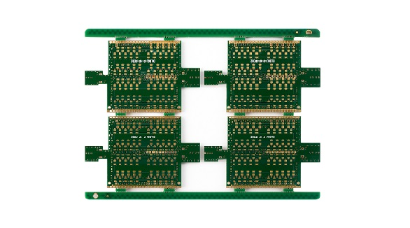
Tab routing is a fabrication technique where multiple PCBs remain connected within a single panel during various manufacturing stages. Instead of fully cutting the boards apart, small tabs—typically a few millimeters wide—are strategically left in place. These tabs secure the individual PCBs, allowing for their separation later, usually after the entire PCB assembly process is completed.
This approach proves especially beneficial in automated assembly environments, where high-speed machinery processes panels of PCBs for component placement and soldering. By maintaining the boards' connectivity, tab routing ensures stability throughout these critical stages, minimizing risks of misalignment or damage. It is a favored technique in Surface Mount Technology (SMT) assembly, where precise component placement is crucial for dense board designs.
Key Advantages of Implementing Tab Routing in PCB Assembly
The benefits of tab routing are extensive, influencing everything from manufacturing costs to product quality. These advantages underscore why tab routing has become an indispensable technique in contemporary PCB assembly processes.
Boosting Efficiency in Automated Assembly
In automated assembly lines, speed and precision are paramount. Tab routing enables the processing of multiple PCBs as a single unit, drastically reducing the time spent on handling individual boards. For instance, a panel containing numerous small PCBs can be processed through a pick-and-place machine in one go, potentially cutting setup time by up to 50% compared to processing each board separately. This efficiency is a significant gain for high-volume production utilizing advanced PCB manufacturing equipment.
Enhancing Accuracy in SMT Assembly
During SMT assembly, miniature components, sometimes as small as 0.4mm x 0.2mm (0402 size), are placed with extreme accuracy. Any movement or misalignment can lead to critical defects. Tab routing stabilizes the panel, ensuring that boards do not shift during component placement or soldering. This stability can reduce placement errors by a notable margin, according to industry benchmarks.
Reducing Manufacturing Costs
Separating boards early in the production cycle often necessitates additional manual labor or specialized tools, which drives up expenses. Tab routing minimizes the need for extra handling; the tabs can be easily broken manually or with simple tools post-assembly. This can lead to a significant reduction in overall production costs, varying with volume and board complexity.
Mitigating Damage Risks
Individual PCBs are inherently more susceptible to bending, cracking, or edge damage during handling. Tab routing keeps them securely attached within the panel, offering protection to delicate edges and traces. For boards with thin substrates (e.g., 0.8mm thick), this additional protection can substantially decrease damage rates.
Facilitating Custom Design Flexibility
Tab routing is highly adaptable to a wide array of board shapes and sizes, making it an ideal choice for custom or irregularly shaped designs. Whether producing standard rectangular boards or complex forms for IoT devices, tab routing optimizes the panel layout, maximizing material usage and potentially reducing waste.
A Step-by-Step Walkthrough of Tab Routing in PCB Assembly
Understanding the practical application of tab routing can help integrate it effectively into your PCB assembly process. Here’s a detailed guide for engineers and manufacturers aiming to optimize their workflow with automated and SMT assembly.
Step 1: Designing the Panel Layout
The process commences with the panel layout design using PCB design software. Engineers arrange multiple PCBs on a single panel, allocating space for tabs—typically 2-3mm wide—between individual boards. The number of tabs per board, generally 3-5, depends on the board's size and weight. Crucially, tab placement must avoid interference with critical components or traces near the board edges. Modern PCB design tools often feature simulation capabilities to optimize tab locations and minimize stress points.
Step 2: Panel Fabrication with Tabs
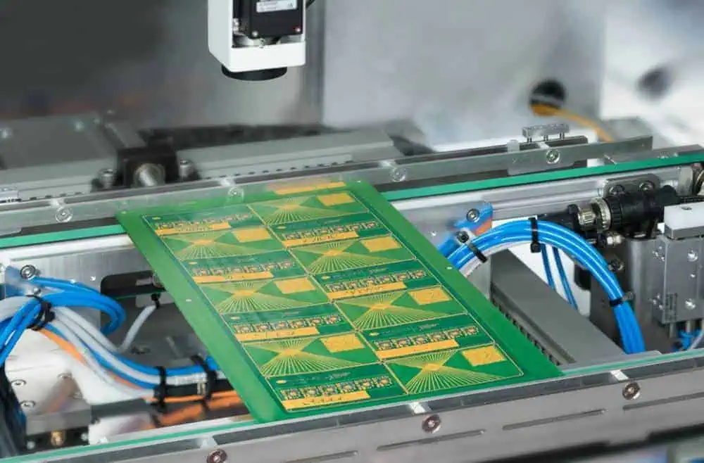
Following design finalization, the panel is fabricated with the tabs incorporated. During this stage, manufacturers employ CNC routers or lasers to cut the outline of each PCB, intentionally leaving the small tabs to maintain panel integrity. The precision of contemporary PCB manufacturing equipment ensures cuts are accurate, preventing weak or improperly placed tabs.
Step 3: Component Placement in SMT Assembly
Once fabricated, the panel moves to the SMT assembly line. Automated pick-and-place machines install components onto all boards in the panel during a single pass. The tabs ensure precise board alignment, facilitating high-precision component placement—often within stringent tolerances. This step is vital for upholding quality in high-density designs.
Step 4: Soldering and Reflow Process
After component placement, the panel undergoes soldering, typically in a reflow oven as part of SMT assembly. The tabs prevent board shifting during this high-temperature process, which can reach 260°C for lead-free solder. This stability effectively reduces defects such as tombstoning or solder bridging by maintaining consistent alignment.
Step 5: Testing and Inspection
Before the boards are separated, the entire panel undergoes functional testing. Automated Optical Inspection (AOI) systems detect soldering defects, while In-Circuit Testing (ICT) verifies electrical performance. Keeping boards panelized during testing simplifies handling and minimizes the risk of damage to individual units.
Step 6: Depaneling (Board Separation)
Upon completion of assembly and testing, individual PCBs are separated from the panel by breaking or cutting the tabs. This can be executed manually for low-volume production or by automated depaneling machines for larger runs. The process is designed to yield clean edges, with modern equipment achieving high edge smoothness.
Tab Routing and Its Synergy with Modern PCB Manufacturing Equipment
The efficacy of tab routing in the PCB assembly process is closely linked to continuous advancements in PCB manufacturing equipment. Today’s automated systems are specifically engineered to handle panelized boards with exceptional precision, making tab routing more effective than ever.
For example, high-speed pick-and-place machines can process panels at impressive rates, relying on the stability provided by tab routing to maintain accuracy across large arrays of boards. Similarly, advanced depaneling tools, such as laser cutters or specialized routers, separate boards without inducing material stress, ensuring clean edges even on thin substrates. This symbiotic relationship between tab routing and automated assembly equipment reduces downtime and significantly boosts production cycle times in high-volume settings.
Key Challenges and Important Considerations for Tab Routing
While the advantages of tab routing are substantial, certain challenges and considerations must be addressed during the design and manufacturing phases to ensure optimal outcomes.
One potential concern is the stress imparted on the board during depaneling. If tabs are excessively thick or improperly placed, breaking them can induce micro-cracks in the PCB, especially near sensitive edge-mounted components. To mitigate this, tabs should be designed with appropriate thickness (e.g., no more than 0.5mm for standard FR-4 material) and strategically located away from critical areas. Another factor is the space required for the tabs themselves. In highly dense panels, allocating this space might slightly reduce the number of boards per panel, potentially increasing material costs. However, this trade-off is often justified by the significant efficiency gains in automated assembly.
Integrating Tab Routing into Your PCB Assembly Strategy
For manufacturers and engineers seeking to optimize their PCB assembly processes, tab routing presents a proven and highly effective solution. Its capacity to enhance efficiency, reduce costs, and improve overall quality makes it an invaluable tool for both small-scale and high-volume production scenarios.
When undertaking projects with tight deadlines or complex designs, integrating tab routing into your workflow is highly recommended. Collaborating closely with your manufacturing partner is key to designing panel layouts that fully leverage the benefits of tab routing, ensuring tabs are positioned for maximum stability without compromising board functionality. Furthermore, utilizing advanced PCB manufacturing equipment designed for panelized assembly and precise depaneling can further amplify the advantages of this technique.
The Transformative Impact of Tab Routing on PCB Assembly
Tab routing has undeniably revolutionized the PCB assembly process, offering a straightforward yet potent method to significantly boost both efficiency and product quality. From streamlining automated assembly lines to enhancing precision in SMT assembly, its widespread benefits are fundamentally reshaping modern manufacturing approaches. As PCB manufacturing equipment continues to evolve and advance, tab routing will remain a cornerstone technique, essential for meeting the increasingly demanding requirements of contemporary electronics production. AIVON is committed to providing expertise and solutions to help integrate such advanced techniques into your manufacturing workflow.


