Introduction
In PCB manufacturing, the application of solder paste during surface mount technology assembly demands exceptional control to ensure reliable solder joints. Laser-cut stencils have become a cornerstone in this process, offering unmatched precision for depositing solder paste onto pads. These stencils enable engineers to achieve consistent results across high-density boards, minimizing defects like bridging or insufficient paste volume. Factory operations increasingly rely on them for fine-pitch components, where even minor inaccuracies can lead to assembly failures. This article explores the laser cutting process for stencils, their advantages, and key factors influencing stencil precision and accuracy.
What Are Laser-Cut Stencils and Why Do They Matter
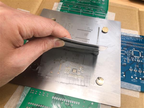
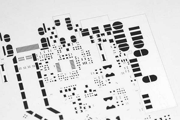
Laser-cut stencils consist of thin metal foils, typically stainless steel, with precisely cut apertures that match the PCB pad layout. The laser cutting process vaporizes material to form these openings, producing smooth walls essential for clean solder paste release. In contrast to chemical etching, which can leave tapered edges, laser-cut stencils provide vertical sidewalls for better paste transfer. They matter in modern PCB manufacturing because high-component densities require tolerances down to microns, directly impacting yield rates in production lines. Engineers value them for supporting miniaturization trends in electronics, ensuring assemblies meet performance specifications under thermal and mechanical stresses.
Adherence to standards like IPC-7525 for stencil design guidelines ensures compatibility across manufacturing facilities. These stencils facilitate step-down or multi-level features for mixed component heights, optimizing paste volume control. Without precise stencils, variability in paste deposition leads to rework, increasing cycle times and costs.
The Laser Cutting Process for Stencils
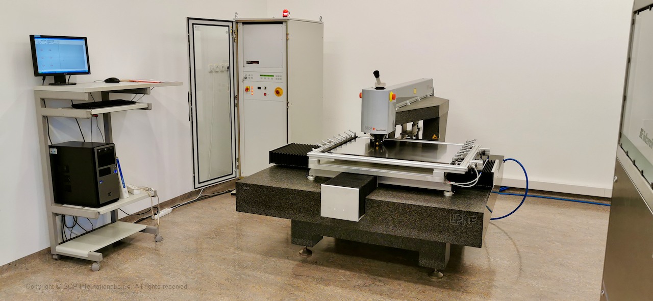
The laser cutting process for stencils begins with loading a foil sheet into a specialized laser system programmed from Gerber data. A high-power laser beam, often fiber or CO2 type, focuses on the material surface, ablating it layer by layer to create apertures. This ablation occurs in a controlled environment to manage debris and heat-affected zones, resulting in crisp edges without burrs. Post-cutting, electropolishing refines the surfaces, enhancing paste release by smoothing walls and reducing surface tension.
Process parameters such as beam power, pulse duration, and scan speed determine cut quality, with factories calibrating systems for specific foil thicknesses ranging from 75 to 150 microns. Alignment fiducials on the stencil frame ensure registration accuracy during printing. The entire process typically completes in hours, far quicker than etching methods, supporting rapid prototyping and volume production.
Laser Cut Stencil Advantages
Laser cut stencil advantages include superior edge quality and repeatability, critical for fine-pitch QFN, BGA, and 01005 components. The vertical aperture walls promote complete solder paste withdrawal, reducing defects compared to etched stencils with undercuts. Factories report higher first-pass yields, as the process allows complex geometries like trapezoidal apertures for improved paste flow. Durability extends stencil life over thousands of prints, lowering long-term maintenance needs.
Another key benefit lies in design flexibility, enabling nano-coatings or hybrid features without compromising integrity. Production speed accelerates time-to-market, vital for iterative designs in engineering workflows. Overall, these advantages align with demands for higher circuit densities and reliability in harsh environments.
Stencil Precision and Accuracy Explained
Stencil precision refers to the consistency of aperture dimensions and positions relative to design files, often achieving tolerances below 25 microns. Accuracy measures how closely the cut matches the intended pad layout, influenced by laser optics and motion control systems. In PCB manufacturing, these metrics ensure solder paste volumes align with IPC-7525 area ratio recommendations, typically above 0.66 for reliable transfer. Variations beyond specified limits cause bridging on dense pads or voids under components.
Factory-driven quality control involves laser interferometry for measuring aperture widths and registration errors post-fabrication. Environmental factors like temperature fluctuations affect foil stability, necessitating controlled cleanrooms. Engineers prioritize stencils where precision supports 0.3mm pitch assemblies without compromising joint integrity.
Factors Influencing Stencil Precision and Accuracy
Foil material selection impacts precision, with high-grade stainless steel resisting warping during cutting. Laser wavelength and focus depth control heat input, preventing microcracks that degrade accuracy over time. Software compensation for beam divergence ensures positional fidelity across large panels.
Stencil thickness interacts with aperture size, where thinner foils enhance precision for micro-components but demand tighter tolerances. Post-processing like electropolishing reduces residue buildup, maintaining accuracy through print cycles. Adhering to J-STD-001 requirements for soldering materials further validates stencil performance in assembly validation.
Handling and storage protocols minimize distortions, as fingerprints or improper tensioning alter flatness. Regular machine calibration sustains these factors in high-volume factories.
Laser Cut Stencil Cost Considerations
Laser cut stencil cost balances initial fabrication with operational efficiencies, generally higher than etched but lower than electroformed options. Economies arise from rapid turnaround, reducing inventory holding for prototypes. Factories amortize costs over extended stencil lifetimes, offsetting premium pricing through fewer replacements.
Volume production lowers per-unit expenses via optimized nesting of designs on foil sheets. Custom features like step stencils increase costs due to multi-pass cutting, yet justify for mixed-technology boards. Engineers evaluate total cost of ownership, factoring yield improvements that cut rework expenses.
Best Practices for Laser-Cut Stencils in Manufacturing
Select stencil thickness based on smallest aperture, aiming for 1:1 to 1:1.5 ratios per IPC guidelines to optimize paste release. Incorporate fiducials and tooling holes for sub-10-micron alignment during printing. Validate designs with simulation software predicting transfer efficiency before cutting.
Implement nano-coatings for hydrophobic surfaces, enhancing cleanability and precision retention. Perform print trials on test boards to fine-tune pressure and speed parameters. Store stencils flat in sealed environments to preserve accuracy.
Regular audits of laser systems ensure consistent stencil quality across runs.
Conclusion
Laser-cut stencils deliver the precision and accuracy essential for advanced PCB manufacturing, streamlining solder paste application in high-density assemblies. Their advantages in edge quality, speed, and reliability outweigh modest cost premiums for most applications. By following standards like IPC-7525, engineers achieve repeatable results that boost yields and reliability. Integrating best practices ensures these tools meet evolving demands in electronics production.
FAQs
Q1: What are the main laser cut stencil advantages over etched stencils?
A1: Laser cut stencil advantages include smoother, vertical aperture walls for better solder paste release and higher precision for fine-pitch components. They offer faster production times and longer lifespan, reducing defects in dense PCB layouts. Factories achieve superior yields without undercuts common in etching, aligning with IPC-7525 guidelines for reliable joints. Overall, they balance performance and cost for most SMT processes.
Q2: How does the laser cutting process for stencils ensure high stencil precision?
A2: The laser cutting process for stencils uses focused ablation to create micron-level apertures with vertical walls, ensuring stencil precision. Controlled parameters like pulse energy and scan speed minimize thermal distortion. Post-processing electropolishing refines surfaces for consistent paste transfer. This method supports tolerances critical for 0.3mm pitch assemblies in manufacturing.
Q3: What factors affect stencil accuracy in PCB manufacturing?
A3: Stencil accuracy depends on foil quality, laser calibration, and environmental controls to prevent warping. Aperture design per IPC-7525 maintains positional fidelity and area ratios above 0.66. Handling practices and fiducial alignment further enhance registration during printing. These elements ensure reliable solder joints across production runs.
Q4: Is laser cut stencil cost justified for high-volume production?
A4: Laser cut stencil cost proves justified through rapid fabrication and durability over thousands of prints, lowering total ownership expenses. Higher upfront fees yield better precision, reducing rework in fine-pitch boards. Compared to alternatives, efficiencies in yield and speed make them economical for factories handling complex designs.
References
IPC-7525 — Stencil Design Guidelines. IPC
J-STD-001 — Requirements for Soldered Electrical and Electronic Assemblies. IPC, JEDEC


