Introduction
Lead-free assembly certification ensures that printed circuit boards and their components meet environmental regulations and reliability standards for soldering without lead. This certification process verifies compliance with directives that restrict hazardous substances, making it essential for global market access. PCB designers must understand these requirements early to avoid costly redesigns during manufacturing. The shift to lead-free processes demands adjustments in materials, processes, and design rules due to higher soldering temperatures. By focusing on lead-free PCB design rules and related practices, engineers can achieve robust assemblies that perform reliably in demanding applications.
What Is Lead-Free Assembly Certification and Why It Matters
Lead-free assembly certification confirms that the entire PCB assembly process, from board fabrication to final soldering, avoids lead and other restricted materials. It typically involves audits, testing, and documentation aligned with industry consensus standards to prove compliance. For PCB designers, this certification matters because it influences material choices, thermal management, and manufacturability from the schematic stage onward. Non-compliance can lead to rejected products, supply chain disruptions, or field failures from incompatible components. In high-volume production, certified processes reduce defects like tombstoning or head-in-pillow issues common in lead-free reflow. Ultimately, embracing these practices supports sustainability while maintaining electrical performance.
Key Technical Principles of Lead-Free Assembly
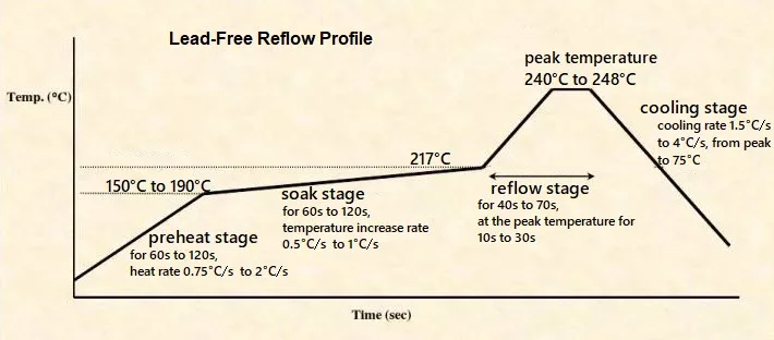
Lead-free soldering relies on alloys with higher melting points, typically around 217 degrees Celsius to 220 degrees Celsius, compared to traditional tin-lead solders. This requires reflow profiles with peak temperatures up to 260 degrees Celsius, stressing boards, components, and joints more intensely. Thermal expansion mismatches between materials can cause warpage, delamination, or microcracks if not addressed in design. Designers must account for these principles by selecting laminates with elevated glass transition temperatures above 170 degrees Celsius. Proper preheat and soak times in the reflow oven help control liquidity and wetting without overheating sensitive parts. Understanding these mechanisms prevents common pitfalls like incomplete solder joints or component damage.
Lead-Free PCB Design Rules
Lead-free PCB design rules prioritize thermal stability and mechanical integrity under elevated process temperatures. Increase copper weights to 2 ounces per square foot or thicker to improve heat dissipation and reduce thermal gradients across the board. Specify via plating thicknesses that withstand multiple reflow cycles without barrel cracking, typically 25 microns minimum. Adjust pad sizes and clearances for better solder flow, ensuring annular rings remain at least 0.15 millimeters after etching. Incorporate thermal relief patterns on pads connected to large planes to avoid solder starvation during reflow. These rules minimize risks like pad lifting or via failures observed in high-temperature processes.
For multilayer boards, route high-current traces on inner layers to leverage the board's mass for heat sinking. Avoid sharp corners in polygons that could concentrate stress during thermal cycling. Simulate warpage using finite element analysis early to predict bow and twist below 0.75% as per qualification specs. Balance copper distribution across layers to prevent uneven heating. These structured approaches ensure the PCB endures lead-free assembly without compromising signal integrity.
Lead-Free Component Selection
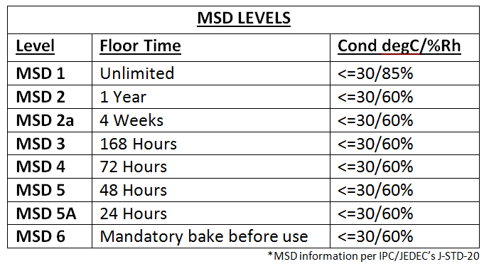
Lead-free component selection starts with verifying finishes like matte tin or pure tin to ensure compatibility with high-temperature soldering. Components must carry markings indicating lead-free status, helping assemblers avoid mixed processes. Check moisture sensitivity levels classified under JEDEC J-STD-020 to match reflow profiles and prevent popcorn effects. Prioritize parts rated for at least three reflow cycles at peak temperatures above 250 degrees Celsius. Passive devices like resistors and capacitors often need high-temperature terminations to resist leaching. Active devices, such as ICs in BGA packages, require underfill considerations for reliability post-assembly.
Troubleshoot selection by reviewing datasheets for alloy compatibility and thermal limits. Avoid components with pure tin plating over 10 microns thick due to whisker growth risks over time. Group parts by reflow sensitivity during placement to optimize oven profiles. Test samples in simulated lead-free conditions to validate joint strength. This methodical process reduces assembly defects and extends product lifespan.
Lead-Free Solder Paste Recommendations
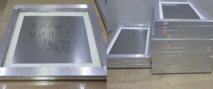
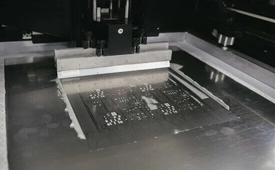
Lead-free solder paste recommendations focus on tin-silver-copper alloys for their reliable wetting and joint formation. Select pastes with particle sizes type 4 or finer for fine-pitch components to achieve uniform deposits. No-clean formulations minimize residue issues while providing flux activation up to 250 degrees Celsius. Ensure metal loading around 88% to 92% for optimal slump resistance during printing. Viscosity should suit stencil thicknesses of 0.1 to 0.125 millimeters for high yields. These choices support consistent reflow without bridging or insufficient solder volume.
In practice, validate paste with printer trials to check release from stencils above 75%. Store paste at 5 to 10 degrees Celsius and allow acclimation before use to prevent printing defects. Monitor shelf life closely, typically six months refrigerated. Adjust reflow parameters based on paste datasheets for peak activation. Proper recommendations troubleshoot voids and enhance lead-free assembly DFM.
Lead-Free Assembly DFM Considerations
Lead-free assembly DFM emphasizes process windows widened by higher temperatures and alloy behaviors. Optimize stencil apertures to 100% to 125% of pad size for QFNs and BGAs to compensate for reduced wetting. Use step stencils for height differences between fine-pitch and larger parts to avoid solder starvation. Implement nitrogen reflow atmospheres to improve joint cosmetics and reduce oxidation. Control ramp rates below 3 degrees Celsius per second to prevent thermal shock. These DFM practices cut rework rates significantly.
Placement accuracy tightens to plus or minus 25 microns for 0.3-millimeter pitch devices under IPC J-STD-001 guidelines. Verify solder paste inspection post-print to catch volume variations early. Profile ovens with thermocouples on test boards matching production stackups. Post-reflow X-ray analysis detects hidden voids promptly. Integrating these steps streamlines certification and boosts first-pass yields.
High-Temperature PCB Design Strategies
High-temperature PCB design for lead-free reflow demands materials with glass transition temperatures exceeding 170 degrees Celsius to resist softening. Specify laminates meeting IPC standards for dimensional stability under thermal stress. Thicken cores and prepregs to distribute heat evenly and curb warpage. Embed thermal vias under hot components to channel heat away from solder joints. Use controlled impedance traces with wider widths to handle current without excessive heating. These strategies safeguard integrity during peak exposures.
Layer sequencing influences thermal paths, so position power planes near surfaces for better cooling. Incorporate fiducials oversized for high-temp alignment shifts. Simulate CTE mismatches to predict reliability in field use. Balance panel arrays with dummy coupons for uniform processing. Troubleshooting involves bow and twist measurements post-bake to validate designs.
Troubleshooting Common Lead-Free Assembly Issues
Tombstoning occurs from rapid heating causing uneven pad melting, resolved by symmetric pad designs and slower ramps. Head-in-pillow defects stem from insufficient flux or mismatched reflow, fixed with optimized profiles and paste selection. Solder beading results from excess paste volume, addressed via precise stencil reductions. Inspect joints visually and with AOI against class 2 or 3 criteria. Rework follows guidelines to avoid damaging surrounding areas. Systematic troubleshooting maintains certification compliance.
Conclusion
Lead-free assembly certification requires PCB designers to integrate specific rules, component choices, and DFM from the outset. By applying high-temperature design principles and standards like JEDEC J-STD-020 and IPC J-STD-001, engineers ensure reliable, compliant products. Practical recommendations for solder paste and troubleshooting further enhance manufacturability. These efforts not only meet regulatory demands but also improve long-term performance. Designers prioritizing these aspects streamline production and reduce risks effectively.
FAQs
Q1: What are the main lead-free PCB design rules for high-temperature processes?
A1: Lead-free PCB design rules include using high-Tg laminates above 170 degrees Celsius, thicker copper for heat management, and thermal reliefs on pads. Balance copper distribution to minimize warpage and ensure via plating withstands multiple reflows. Simulate thermal profiles early to predict issues. These rules support robust assembly under 260-degree Celsius peaks.
Q2: How do I perform lead-free component selection effectively?
A2: Verify components have lead-free finishes and MSL ratings per JEDEC J-STD-020 for your reflow profile. Prioritize parts enduring three cycles above 250 degrees Celsius. Review markings and test samples for joint reliability. Group by sensitivity during assembly to optimize processes.
Q3: What lead-free solder paste recommendations improve DFM?
A3: Choose tin-silver-copper pastes with type 4 particles, 88-92% metal loading, and no-clean flux for fine-pitch work. Match viscosity to 0.1-millimeter stencils and validate printing yields. Acclimate paste before use and profile reflow accordingly for minimal defects.
Q4: Why is high-temperature PCB design critical for lead-free assembly?
A4: High-temperature PCB design counters reflow peaks up to 260 degrees Celsius that stress materials beyond standard limits. High-Tg boards prevent delamination, while thermal vias and plane placement manage heat. This ensures mechanical stability and electrical performance post-assembly.
References
IPC J-STD-001 — Requirements for Soldered Electrical and Electronic Assemblies. IPC, 2020
JEDEC J-STD-020E — Moisture/Reflow Sensitivity Classification for Nonhermetic Surface Mount Devices. JEDEC, 2014
IPC-6012E — Qualification and Performance Specification for Rigid Printed Boards. IPC, 2017