What Are SMD Components and 3D Printed PCBs?
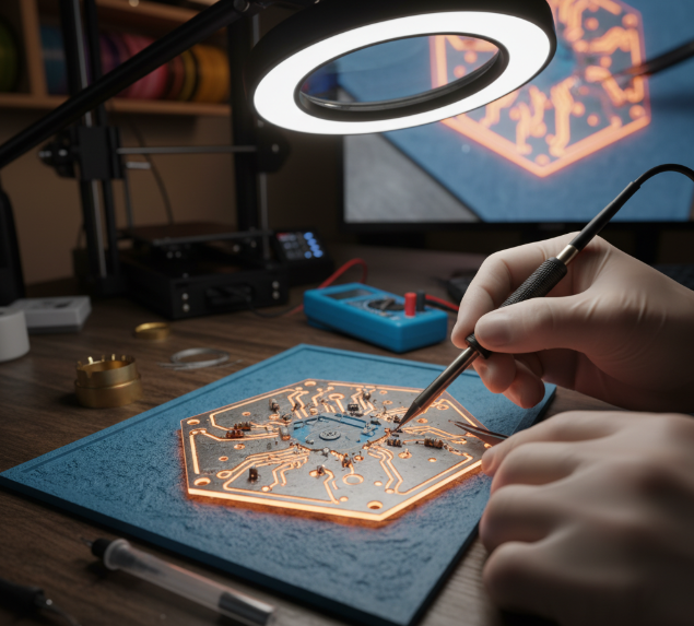
Venturing into electronics projects often involves navigating the intricacies of soldering, especially when dealing with the miniature world of Surface-Mount Device (SMD) components. Unlike traditional through-hole parts that require leads to be inserted into drilled holes, SMDs are designed for direct soldering onto the circuit board's surface. Their compact size makes them indispensable for modern, space-efficient electronic designs.
On the other hand, 3D printed PCBs represent a custom approach to circuit board fabrication, leveraging additive manufacturing. Instead of conventional methods, these boards can be designed and printed using specialized conductive filaments or inks, or even created as a non-conductive base onto which conductive paths are manually applied. This technology is particularly valuable for rapid PCB prototyping and DIY electronics projects, offering unparalleled flexibility and creative freedom. The integration of SMD soldering with 3D printed PCBs empowers hobbyists and engineers to develop highly customized, lightweight, and innovative electronic solutions.
Advantages of Using 3D Printed PCBs for SMD Soldering
While conventional PCBs are optimized for PCB mass production, 3D printed PCBs offer distinct benefits, especially for beginners and hobbyists engaged in DIY electronics projects.
Flexibility and Efficiency for Prototyping
● Customization: 3D printing allows for the creation of PCBs in virtually any shape or size using 3D modeling software, making them ideal for unconventional or specialized project enclosures.
● Rapid Prototyping: The ability to print a board in mere hours significantly reduces development time, eliminating the days or weeks typically spent waiting for conventionally manufactured boards.
● Cost-Effectiveness for Small Batches: For one-off designs or small production runs, 3D printed PCBs offer a cost-effective alternative to the higher setup costs associated with traditional PCB fabrication.
● Learning Platform: Experimenting with 3D printed PCBs provides a low-risk environment for beginners to learn SMD soldering techniques and test new circuit ideas without the fear of damaging expensive, pre-made boards.
Limitations to Consider
It is important to acknowledge that 3D printed PCBs often have limitations compared to their copper-clad counterparts. Their conductivity is typically much lower (e.g., 0.1-1 S/m for conductive filaments versus 5.96 × 10^7 S/m for copper). Additionally, they may exhibit reduced durability under high temperatures, which makes precision and careful heat management during the soldering process even more critical.
Essential Tools and Materials for SMD Soldering on 3D Printed PCBs
To embark on your SMD soldering journey with 3D printed PCBs, gathering the correct tools and materials is crucial. This comprehensive list is tailored specifically for beginners:
● Soldering Iron: A fine-tip soldering iron (15-30W) with adjustable temperature control is ideal. For SMD work, set the temperature between 260-300°C to prevent damage to components or the 3D printed material.
● Solder: Use lead-free solder wire with a fine diameter (0.5-0.8mm) for precision work.
● Flux: A no-clean flux pen is recommended for ease of use. Flux aids in solder flow and prevents oxidation, ensuring stronger joints.
● Tweezers: Precision tweezers are indispensable for accurately handling and placing tiny SMD components.
● Magnification: A magnifying glass or a low-power microscope is essential for clearly viewing small pads and components.
● Desoldering Braid: This tool is invaluable for correcting errors by efficiently removing excess solder.
● 3D Printer and Filament: A 3D printer for fabricating the PCB base. Standard PLA or PETG filaments are suitable for the structural base, while specialized conductive filaments can be used for embedded traces.
● Conductive Paint or Ink: If your 3D printer does not support conductive filament, use this to manually draw conductive traces on the printed board.
● Multimeter: A multimeter is necessary for testing connections, verifying continuity, and checking for short circuits after soldering.
● SMD Components: A selection of common SMD components such as resistors, capacitors, LEDs, or integrated circuits (ICs), depending on your specific project.
Step-by-Step Guide: SMD Soldering on 3D Printed PCBs
With your tools prepared, let's proceed with the process of soldering SMD components onto a 3D printed PCB. Adhering to these steps carefully will yield the best results.
Design and Print Your PCB
Begin by designing your circuit layout using software such as KiCad or Fritzing. If you intend to print the board structure, export your design as a 3D model. Ensure that the pads for SMD components are appropriately sized (typically 0.8-1.2mm wide for smaller components like 0805 resistors). Print the PCB using your 3D printer. If you are using conductive filament, ensure the traces are accurately aligned during printing. If not, print a non-conductive base and prepare to add conductive paths manually. For smoother surfaces conducive to soldering, maintain a low layer height (around 0.1-0.2mm).
Creating Conductive Traces
If your 3D printed PCB lacks embedded conductive traces, apply conductive paint or ink to draw the circuit paths. Use a fine brush or pen to ensure even coverage. Allow the paint to dry completely (which usually takes 1-2 hours) before proceeding. Test the newly created traces with a multimeter to confirm conductivity, aiming for a resistance below 10 ohms per centimeter for reliable performance.
Preparing Your Soldering Station
Set your soldering iron to a temperature of 260-280°C for most SMD components. Temperatures exceeding 300°C risk melting the 3D printed material, especially PLA, which has a melting point between 180-220°C. Clean the iron tip with a damp sponge or brass wire cleaner to remove any residue. Apply a small amount of flux to the PCB pads where components will be placed. Flux enhances solder adhesion and significantly reduces the likelihood of cold joints, which can compromise connection reliability.
Component Placement and Soldering
Using precision tweezers, carefully position the SMD component onto the prepared pads. For a two-lead component like a resistor or capacitor, follow these steps:
1. Apply a small dab of solder to one of the pads.
2. Position the component onto the pads, ensuring one end aligns with the pre-soldered pad.
3. Heat the pre-soldered pad and gently guide the component end into the molten solder. Hold it steady until the solder solidifies (typically 2-3 seconds).
4. Solder the opposite end by simultaneously applying solder wire and the iron tip to the pad and the component lead. Be conservative with solder to prevent unintended bridging.
For larger components with multiple pins, such as ICs, first anchor the component by soldering one corner pin, then proceed to solder the remaining pins. Minimize heat exposure, limiting contact to 1-2 seconds per pin, to prevent damage to the 3D printed base material.
Inspection and Functional Testing
After completing the soldering, meticulously inspect each joint under magnification. Look for joints that appear shiny and smooth, free from cracks or bridges between adjacent pads. Use a multimeter to test for continuity between connected points and to confirm the absence of any short circuits. Should you identify an error, use desoldering braid and a fresh application of flux to remove excess solder. Once removed, you can then reposition or replace the component as necessary.
Practical Tips for Successful SMD Soldering on 3D Printed PCBs
Soldering miniature components onto a non-traditional board can be intricate. Here are several practical tips to enhance your results in DIY electronics projects:
● Ventilate Your Workspace: Soldering produces fumes; ensure adequate ventilation or use a fume extractor.
● Prioritize Practice: Before commencing work on your actual project, practice soldering SMD components on a scrap piece of material or a dedicated test PCB.
● Consider Low-Melting-Point Solder: If your 3D printed PCB material is particularly heat-sensitive, using solder with a lower melting point (around 180-200°C) can significantly reduce the risk of thermal damage.
● Secure Components: For multi-pin parts or to prevent shifting, apply a small dot of adhesive or a piece of double-sided tape to temporarily secure components in place before soldering.
● Prevent Overheating: Limit the duration of soldering iron contact on each joint to prevent warping or melting the printed board. Allow the board to cool between soldering sessions if prolonged work is required.
Common Challenges and Troubleshooting in 3D Printed PCB Soldering
Beginners frequently encounter obstacles when learning how to solder SMD components onto 3D printed PCBs. Here are some common issues and their corresponding solutions:
● Warped or Melted PCB: This typically occurs if the soldering iron is too hot or applied for an extended period. Use a lower temperature (around 260°C) and work with greater speed. If warping persists, consider reprinting the board using a more heat-resistant material like PETG.
● Poor Trace Conductivity: Conductive paints or filaments often exhibit higher resistance than traditional copper. Double-check all connections with a multimeter and, if necessary, reinforce weak traces with additional layers of conductive material.
● Solder Bridges: When solder inadvertently connects two adjacent pads, use desoldering braid to absorb the excess. Applying flux beforehand can often help prevent this issue from occurring.
● Component Misalignment: SMD components are tiny and can easily shift during the soldering process. Use tweezers for precise placement and ensure they are securely positioned before applying solder.
Project Idea: Building a Simple LED Circuit on a 3D Printed PCB
To apply and test your newly acquired skills, consider building a straightforward LED blinker circuit using SMD components on a 3D printed PCB.
Quick Project Overview
1. Circuit Design: Design a basic circuit incorporating a 555 timer IC, a few SMD resistors (e.g., 1kΩ and 10kΩ in 0805 size), an SMD capacitor (e.g., 0.1μF), and an SMD LED.
2. PCB Fabrication: Print a small rectangular PCB base (e.g., 5cm x 3cm) with ample space for the components.
3. Trace Creation: Either draw or print the conductive traces to connect the components according to your circuit schematic.
4. SMD Soldering: Solder all the SMD components onto the board following the detailed steps outlined earlier in this guide.
5. Power and Test: Apply a 5V power supply to the circuit and observe the LED blinking at a frequency determined by your chosen resistor and capacitor values (typically around 1-2 Hz).
This project serves as an excellent practical exercise for mastering SMD soldering on 3D printed PCBs while simultaneously creating a functional piece of electronics.
Conclusion: Empowering Your Electronics Projects
Mastering SMD soldering on 3D printed PCBs unlocks a vast realm of possibilities for DIY electronics projects. While the initial learning curve might seem steep, with the appropriate tools, refined techniques, and persistent patience, even a beginner can achieve professional-caliber results. This comprehensive soldering tutorial has covered all the essential aspects—from the initial design and 3D printing of your PCB to the intricate process of soldering tiny components and effectively troubleshooting common issues.
Begin with smaller projects, practice consistently, and experiment with diverse designs to progressively build your confidence. As your proficiency in soldering SMD components grows, you will find yourself capable of tackling increasingly complex electronics projects, transforming your creative concepts into tangible realities. Continue to explore, innovate, and let your ingenuity shine through your creations!


