What is Surface Mount Technology (SMT) and Why is Component Placement Crucial?
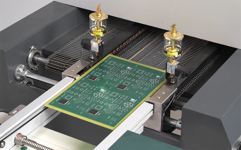
Surface Mount Technology (SMT) is a sophisticated method for mounting electronic components directly onto the surface of a Printed Circuit Board (PCB). Unlike traditional through-hole technology, which necessitates drilling holes for component leads, SMT enables the use of smaller components and allows for significantly denser circuit layouts. This makes SMT ideal for the compact electronic devices prevalent today. However, this increased density also introduces the critical challenge of precise component placement. Inadequate SMT component positioning can lead to various problems, including signal interference, localized overheating, or manufacturing errors during automated assembly.
Proper placement protocols ensure that components are optimally positioned to achieve peak performance, enhance manufacturability, and guarantee reliability. Adhering to robust SMT guidelines is invaluable for both novice and seasoned engineers, as it can drastically reduce development time, cut PCB board cost, and elevate the overall quality of PCB assembly projects.
What Are the Core Principles Guiding SMT Component Layout?
Before delving into specific directives, it is beneficial to understand the fundamental principles that underpin effective SMT component placement. These principles universally aim to optimize functionality, streamline manufacturing, and simplify the assembly process, particularly when employing automated pick-and-place machinery.
● Signal Integrity: Components must be arranged to minimize electronic noise and interference, which is especially critical for circuits handling high-speed signals.
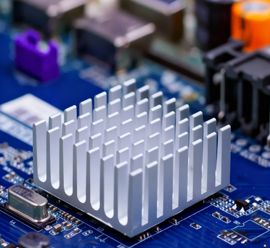
● Thermal Management: Heat-generating parts require adequate spacing to prevent hotspots and ensure efficient heat dissipation throughout the board.
● Manufacturability: Component layout must align with the operational capabilities of automated pick-and-place machines and various soldering techniques.
● Accessibility: Components should be positioned to allow for straightforward inspection, testing, and potential rework if needed after assembly.
With these guiding principles in mind, let’s explore the precise SMT guidelines that contribute to superior surface mount design.
What Are the Essential Rules for SMT Component Placement?
Effective SMT component placement involves several critical rules, each addressing a specific aspect of PCB design and manufacturing. Adhering to these guidelines helps ensure optimal board performance and reliable production.
Maintain Proper Component Spacing
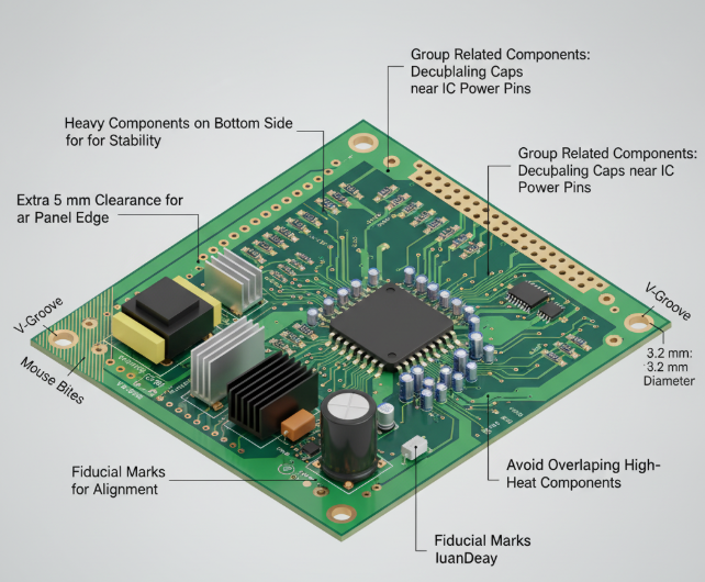
Appropriate spacing between components is paramount in SMT design. Components placed too closely risk soldering defects like bridging, where solder inadvertently connects adjacent pads. Conversely, excessive spacing wastes valuable board real estate. A general guideline suggests a minimum clearance of 0.2 mm (8 mils) between components for standard designs. For high-density layouts, it is crucial to consult your assembly house, as their automated placement machines may have specific tolerances. For example, tiny 0201 resistors (0.6 mm x 0.3 mm) often demand at least 0.1 mm clearance to prevent issues during the reflow soldering process.
Orient Components for Automated Assembly
Automated pick-and-place machines are fundamental to efficient PCB assembly. To facilitate their operation, components should be oriented consistently whenever possible. Aligning diodes, capacitors, and resistors in the same direction, for instance, minimizes machine head rotation during assembly, thereby accelerating production and reducing potential errors. Furthermore, ensuring that component markings, such as polarity indicators on capacitors, are visible and uniform across the board aids in inspection and prevents the incorrect placement of polarized components, which could lead to circuit failure.
Strategically Place High-Speed Components
In designs involving high-speed signals (e.g., above 100 MHz), component placement directly impacts signal integrity. Sensitive components, such as microcontrollers or RF modules, should be positioned close to their associated circuitry to minimize trace lengths. Longer traces can introduce parasitic capacitance and inductance, leading to signal degradation. For example, a mere 10 mm trace can add approximately 50 picoseconds of delay, a significant factor in high frequency PCB applications. Additionally, avoid placing high-speed components near noisy elements like power supplies unless robust shielding or grounding mechanisms are in place. Utilizing ground planes can effectively reduce electromagnetic interference (EMI) and maintain a clean signal path.
Manage Thermal Considerations
Heat dissipation is a critical concern in SMT designs, particularly for power-hungry components like voltage regulators or MOSFETs. Place heat-generating components away from temperature-sensitive parts, such as precision analog ICs, to prevent performance degradation. If feasible, position these components near the board edges or in areas with optimal airflow for enhanced cooling. For instance, a power IC dissipating 2 watts of heat may require a minimum clearance of 5 mm from adjacent components to avoid thermal coupling. Integrating thermal vias or heat sinks near these components can further improve heat management.
What Advanced SMT Guidelines Enhance Complex Designs?
For more intricate PCB designs, several advanced SMT guidelines can further optimize manufacturability and performance. These considerations become particularly important in mass production and double-sided assemblies.
Panelization for Mass Production
In large-scale manufacturing, PCBs are frequently produced in panels containing multiple individual boards. During SMT component placement, it is essential to ensure that components positioned near panel edges have extra clearance, typically at least 5 mm. This additional space accounts for depanelization processes, such as routing or V-scoring, and helps prevent damage to components during the board separation stage. Furthermore, avoiding the placement of tall components close to panel edges is advisable, as they might interfere with assembly equipment or experience uneven mechanical stress during handling.
Optimization for Reflow Soldering
Reflow soldering is the most prevalent method for attaching SMT components to PCBs. To ensure successful and reliable soldering, it is crucial to balance the thermal mass across the board by distributing both large and small components evenly. An imbalanced thermal mass can lead to inconsistent heating during the reflow process, causing defects such as "tombstoning," where one end of a component lifts off its pad. For instance, concentrating large components like transformers on one side while placing tiny 0402 resistors on the other can create temperature differences of up to 20°C during reflow, significantly increasing the risk of soldering issues.
Planning for Double-Sided Assembly
Double-sided SMT designs, where components are mounted on both sides of the PCB, are employed to maximize board space. However, this approach introduces unique assembly challenges. It is generally recommended to place heavier components on the bottom side of the board to prevent them from falling off during the second reflow cycle. Additionally, designers must ensure that components on opposite sides do not overlap in a manner that could induce mechanical stress or lead to localized heat buildup. For example, placing a large IC directly opposite a power resistor on the other side should be avoided, as their combined heat could potentially exceed safe operating temperatures for many components, typically around 85°C.
What Common Pitfalls Should Be Avoided in SMT Component Placement?
Even with meticulous planning, certain common mistakes in surface mount design can lead to costly reworks or even outright board failures. Recognizing and avoiding these pitfalls is critical for successful PCB development.
● Neglecting Design for Manufacturability (DFM): Overlooking DFM guidelines can result in layouts that are either difficult or impossible to manufacture efficiently. Always consult with your assembly partner early in the design phase to understand their specific equipment capabilities and constraints.
● Overcrowding Components: While maximizing space is often desirable, packing components too tightly frequently leads to soldering defects, such as bridging, or errors during automated assembly. Adequate spacing is crucial for reliable manufacturing.
● Ignoring Polarity Markings: Incorrect orientation of polarized components, including diodes or electrolytic capacitors, is a frequent cause of circuit malfunction. Double-checking polarity markings during placement is essential.
● Poor Trace Routing After Placement: Component placement and trace routing should be considered in tandem. Failing to plan routing alongside placement can result in excessively long and noisy traces or an abundance of unnecessary vias, which can degrade signal integrity.
Which Tools and Resources Aid SMT Component Placement?
Modern PCB design software provides invaluable tools to assist with SMT component placement, streamlining the process and reducing errors.
● Automated Placement Algorithms: Many design software packages offer features like auto-placement algorithms that can suggest optimized layouts based on predefined design rules.
● Design Rule Checks (DRC): Built-in DRC functionalities help identify spacing violations, short circuits, and other potential issues before the board is sent for manufacturing, catching problems early saves significant time and cost.
● Manufacturer-Specific Guidelines: Large pcb manufacturer provides detailed Design for Manufacturability (DFM) guidelines tailored to their specific equipment and processes. These resources are invaluable for ensuring a smooth PCB assembly process.
● Industry Standards: Staying current with industry standards, such as those published by the Institute of Printed Circuits (IPC), provides a robust framework for design. For example, the IPC-7351 standard offers comprehensive recommendations for land patterns and component spacing in SMT designs.
Leveraging these tools and resources can significantly enhance the efficiency and reliability of SMT component placement.
Conclusion: Mastering SMT Component Placement for Superior Designs
Effective SMT component placement is a nuanced blend of technical expertise and careful planning, demanding a thorough understanding of both design principles and manufacturing constraints. By meticulously adhering to established SMT guidelines—such as ensuring appropriate spacing, correctly orienting components for automated assembly, and prudently managing thermal considerations—engineers can consistently produce reliable and high-performing PCB layouts.
Whether the project involves a straightforward prototype or a complex, high-density board, these fundamental rules for surface mount design will streamline the PCB assembly process and significantly contribute to overall success. It is highly recommended to allocate sufficient time for meticulous layout planning, strategically utilize available design software tools, and maintain close collaboration with your assembly partner to address any unique project requirements. By integrating these practices, you will be well-equipped to master SMT component placement and consistently deliver top-tier electronic designs.


