Introduction
Wave soldering remains a cornerstone process in PCB assembly for through-hole components, enabling efficient mass production of reliable electronic assemblies. Electrical engineers often rely on this method to achieve consistent solder joints in high-volume manufacturing environments. The wave soldering process involves passing a PCB over a molten solder bath, where precise control of parameters ensures strong mechanical and electrical connections. Understanding its nuances helps mitigate common issues and optimize yield. This guide delves into the mechanics, best practices, and troubleshooting for superior results in through-hole wave soldering.
What Is the Wave Soldering Process and Why It Matters for Through-Hole Components
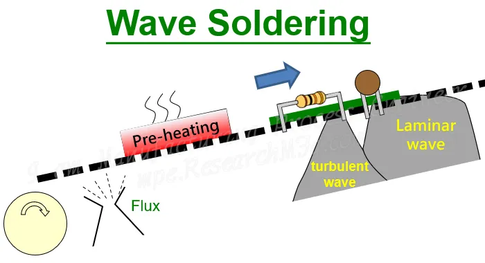
The wave soldering process flux-applies a chemical agent to the PCB underside, preheats the board to activate the flux and prevent thermal shock, then immerses component leads into a turbulent molten solder wave for wetting and solidification. Primarily designed for through-hole technology (THT), it excels in soldering axial, radial, and pin-grid components where leads pass through board holes. Unlike reflow soldering for surface-mount parts, wave soldering leverages gravity and capillary action for hole filling, making it ideal for connectors and high-power devices. Its relevance persists in mixed-technology boards, supporting legacy designs and robust mechanical joints.
Engineers value wave soldering for its speed and cost-effectiveness in medium-to-high volumes, reducing labor compared to hand soldering. Proper execution minimizes rework and enhances reliability in demanding applications like automotive and industrial controls. As boards evolve with denser layouts, mastering this process prevents compatibility issues with surface-mount areas. Adhering to standards like IPC J-STD-001 ensures joints meet performance criteria for vibration and thermal cycling.
Technical Principles of Wave Soldering
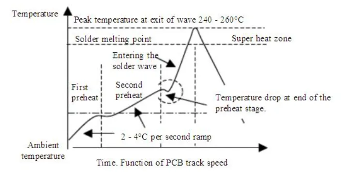
Flux plays a pivotal role by removing oxides from leads, pads, and holes, promoting solder wetting while minimizing surface tension. Common types include no-clean low-solids formulations applied via spray or foam for uniform coverage without post-cleaning needs. During preheating, infrared or hot air raises the PCB temperature to 100-150 degrees Celsius, evaporating flux solvents and expanding holes for better solder entry. This step also reduces thermal gradients that could warp boards or crack components.
The solder pot maintains molten alloy at 250-260 degrees Celsius for lead-free processes, pumped to form a laminar primary wave followed by a turbulent secondary wave. The primary wave wets pads gently, while the secondary ensures thorough hole fill via capillary forces. Conveyor speed, typically 1-2 meters per minute, controls dwell time of 3-5 seconds per wave, balancing fill quality and bridging risk. Cooling fans post-wave solidify joints rapidly, locking in fillet shapes.
Solder alloy choice, often SAC305 for lead-free, influences viscosity and wetting speed. Nitrogen atmospheres in modern machines reduce dross and oxidation, extending pot life. These principles underpin reliable barrel fill exceeding 75% as targeted in process optimization.
Key Parameters in Through-Hole Wave Soldering Temperature and Flux Management
Through-hole wave soldering temperature profiles demand careful tuning: preheat topside at 120-140 degrees Celsius activates flux without degrading components, while solder pot stability at 255 degrees Celsius prevents underheating. Excessive pot temperatures above 270 degrees Celsius accelerate intermetallic growth, weakening joints over time. Flux quantity, around 500-1000 micrograms per square centimeter, ensures activation without splattering. Engineers monitor via dataloggers to maintain preheat slopes below 4 degrees Celsius per second.
Wave soldering flux selection per J-STD-004 categorizes by activity: low (L) for clean assemblies, medium (M) for standard THT. Application uniformity via nozzle pressure avoids shadowing on dense boards. Optimizing these prevents residue that could cause electrochemical migration. Parameter interplay is critical; slower conveyors extend immersion but risk icicles from excess solder drainage.
Common Wave Soldering Defects and Their Root Causes
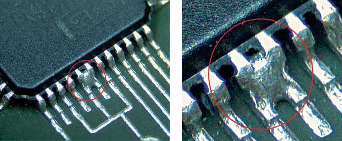
Wave soldering defects like bridging occur when solder spans adjacent pads due to high flux activity or slow conveyor speeds, leading to shorts. Icicles form from prolonged dwell, where viscous solder drips post-wave, violating fillet smoothness. Insufficient hole fill, below 75-100%, stems from inadequate preheat or clogged vias, compromising strength. Solder balls scatter from flux boil-off or turbulence, posing reliability hazards.
Non-wetting shows deoxidized surfaces rejecting solder, often from contaminated flux or cold boards. Dewetting follows initial wetting then retraction due to high surface tension. Pinholes and blowholes arise from trapped gases or moisture in components. IPC-A-610 defines acceptability criteria, classifying these as defects based on joint appearance and fill percentage.
Optimizing Wave Soldering Parameters for Defect-Free Assembly
Start with flux optimization: test spray patterns for even coverage, adjusting volume to match board density. Preheat tuning via thermocouple profiling achieves uniform topside temperatures, minimizing shadows under tall components. Set conveyor angle at 6-8 degrees for optimal drainage, reducing bridges by 50% in trials. Solder pot skimming controls dross, maintaining wave height at 5-10 millimeters.
Dwell time calibration balances fill and defects; shorter for fine-pitch, longer for thick boards. Nitrogen purging at 1000-2000 ppm oxygen enhances wetting without extra cost. Process windows narrow with lead-free alloys, demanding tighter controls. Regular profiling per IPC J-STD-001 verifies compliance.
Fixture design prevents component movement, using pallets for mixed boards. Trial runs with test coupons quantify parameters before production.
Troubleshooting Wave Soldering Issues: Practical Steps
When bridging appears, increase speed or reduce flux, inspecting nozzle clogs first. For poor fill, boost preheat by 10-20 degrees Celsius and verify hole quality. Icicles yield to faster drainage via angle tweaks or wave turbulence adjustment. Solder balls signal flux over-application; switch to low-solids if persistent.
Moisture-related voids require baking components per JEDEC guidelines before insertion. Residue issues post no-clean flux demand activity testing. Log defect Pareto charts to prioritize root causes like parameter drift. Iterative DOE refines setups.
Conclusion
Mastering the wave soldering process for through-hole components hinges on precise parameter control, from through-hole wave soldering temperature to flux selection. Addressing wave soldering defects through systematic troubleshooting elevates assembly yield and reliability. Optimizing wave soldering parameters aligns with standards, ensuring robust joints for electrical engineers. Implement these practices for consistent, high-quality PCB assemblies.
FAQs
Q1: What is the ideal through-hole wave soldering temperature range?
A1: The solder pot typically operates at 250-260 degrees Celsius for lead-free alloys, with preheat reaching 120-150 degrees Celsius topside. These ranges activate flux, promote wetting, and achieve 75-100% hole fill without excessive intermetallics. Monitor profiles to avoid gradients over 4 degrees Celsius per second, reducing warpage and defects. Adjustments depend on board thickness and component density.
Q2: How does wave soldering flux impact the process?
A2: Wave soldering flux removes oxides and lowers surface tension for capillary flow into holes. Low-solids no-clean types per J-STD-004 minimize residues while ensuring wetting. Uniform application via spray prevents shadows and balls. Incorrect flux leads to non-wetting or bridging, so test activity levels for your alloy and board finish.
Q3: What are the most common wave soldering defects and fixes?
A3: Bridging, icicles, and insufficient fill top the list. Speed up conveyor for bridges, angle pallets for icicles, and preheat higher for fill issues. Root causes tie to parameters; profile regularly. IPC-A-610 criteria guide acceptance, targeting zero Class 3 defects.
Q4: How to optimize wave soldering parameters for high-volume production?
A4: Tune preheat, flux volume, speed, and pot temperature iteratively with test boards. Aim for 3-5 second dwell and nitrogen assist. DOE identifies windows, boosting yield over 99%. Standards like IPC J-STD-001 validate joints.
References
IPC J-STD-001G — Requirements for Soldered Electrical and Electronic Assemblies. IPC, 2017
IPC-A-610H — Acceptability of Electronic Assemblies. IPC, 2019
J-STD-004D — Requirements for Soldering Fluxes. IPC/JEDEC, 2011