What challenges arise when routing high-density BGA packages?
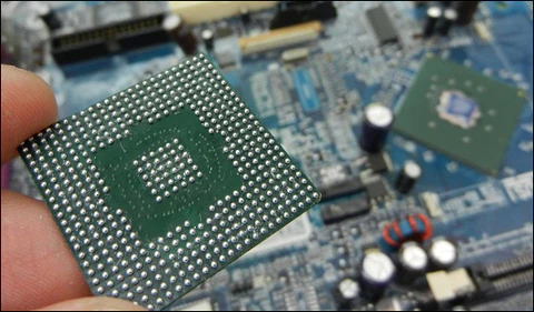
Ball Grid Array (BGA) packages are fundamental in modern electronics, enabling compact designs for microprocessors, FPGAs, and memory. However, their densely packed pins present considerable hurdles for PCB designers, particularly concerning "escape routing"—the process of guiding signals away from BGA pads to other board sections. As pin pitches continue to shrink to 0.5 mm or less and pin counts soar into the thousands, effective escape routing becomes paramount for maintaining signal integrity, ensuring manufacturability, and optimizing performance.
Understanding the complexity
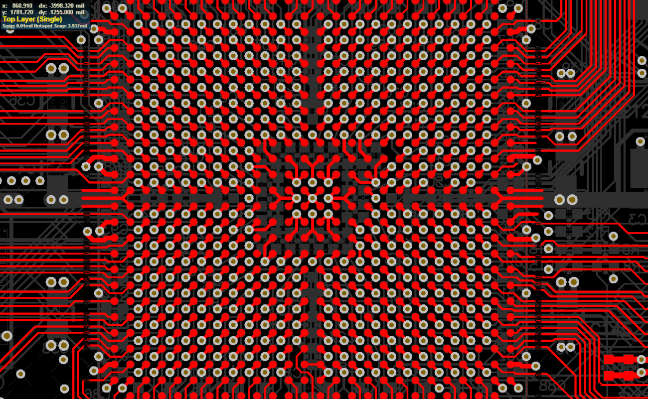
High-density BGA packages, often featuring over 1,000 pins and pitches as fine as 0.4 mm, create a formidable routing environment. The core difficulty lies in extracting signals from this dense grid of solder balls to either the outer layers or internal routing channels of the PCB without introducing congestion, crosstalk, or impedance mismatches. For example, a 0.5 mm pitch BGA with a 40x40 grid contains 1,600 pins, demanding meticulous planning to route each signal while maintaining a trace width of 3 mils or less to prevent overlaps.
Key obstacles designers face
Several critical challenges characterize high-density BGA escape routing. The high pin density severely limits space between pins, often necessitating micro-vias or High-Density Interconnect (HDI) techniques. For high-speed signals, such as DDR4 interfaces operating at 3.2 Gbps, maintaining signal integrity requires controlled impedance (typically 50 ohms) and minimal stub lengths to prevent reflections. Furthermore, routing all signals might demand numerous PCB layers, increasing costs unless optimized. Manufacturing limits also play a role, as trace widths below 3 mils or via sizes smaller than 8 mils can exceed standard fabrication capabilities, requiring advanced processes. To overcome these, engineers must strategically adapt their escape routing techniques based on the BGA's pitch, pin count, and specific signal requirements.
Which escape routing techniques are effective for different BGA pitches?
Addressing the complexities of BGA escape routing involves a range of techniques, each suited to different BGA pitches and design constraints. Choosing the right method is crucial for ensuring successful signal breakout and overall board performance.
Dog-bone fanout for larger pitches
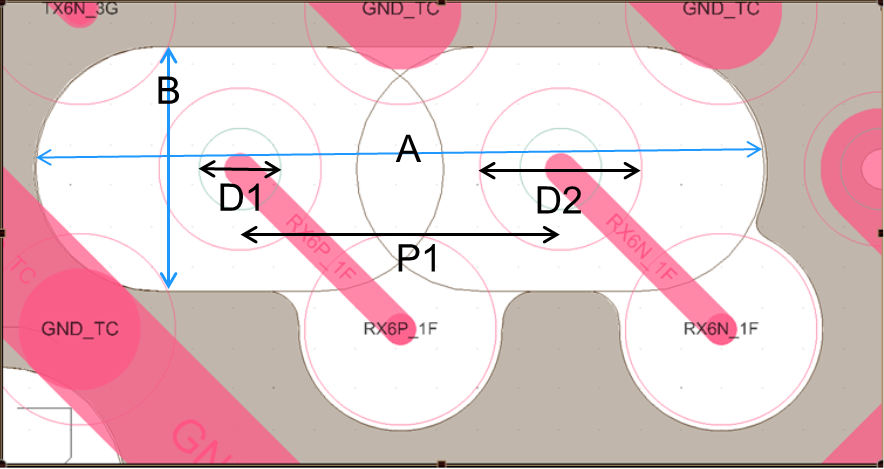
The "dog-bone" fanout is a widely adopted technique for BGAs with pitches of 0.5 mm or greater. In this approach, each BGA pad connects to a via through a short, angled trace, allowing signals to transition to internal PCB layers for further routing. This method proves effective for mid-range pitch BGAs (0.5–1.27 mm) because it provides adequate space to route one or two traces between adjacent pads. Typically, outer rows of BGA pads are routed directly outward, while inner rows utilize vias placed between four adjacent pads, connected by diagonal traces. Trace widths are usually 3–4 mils, with clearances of at least 0.1 mm for a 0.65 mm pitch BGA, ensuring manufacturability. While simple to implement and compatible with standard PCB manufacturing, this technique becomes impractical for pitches below 0.5 mm due to insufficient space.
Via-in-pad for fine-pitch BGAs
For BGAs with pitches below 0.5 mm, "via-in-pad" technology becomes indispensable. Here, vias are placed directly within the BGA pads, filled with conductive or non-conductive epoxy, and then plated over to create a flat surface suitable for soldering. This method maximizes routing space by allowing signals to transition vertically to internal layers. Micro-vias, typically 8 mils in diameter with a 4 mil hole, are drilled directly into the BGA pads and subsequently filled to prevent solder wicking during reflow, ensuring reliable solder joints. Signals are then routed to inner layers, where wider traces (e.g., 5 mils) can be used to reduce resistance. Although this technique significantly increases routing density and is ideal for ultra-fine pitches and HDI designs, it also escalates manufacturing complexity and cost, requiring advanced fast turn PCB fabrication capabilities.
How can advanced routing strategies enhance BGA design?
Beyond basic fanout techniques, integrating advanced strategies like staggered routing, ordered escape, and HDI with micro-vias can significantly optimize BGA designs, particularly for ultra-high-pin-count packages and high-speed applications.
Staggered and ordered escape routing
For intricate designs, staggered or ordered escape routing can streamline signal paths and minimize crossovers. Staggered pin arrays, where pins are offset at 60-degree angles, increase the effective spacing between pads, simplifying trace routing. Ordered escape routing, often managed by algorithms like Min-cost Multi-commodity Flow (MMCF), ensures signals exit the BGA in a predefined sequence to prevent conflicts and optimize flow. This approach allows for wider traces (e.g., 4 mils) between pins, thereby reducing crosstalk, and leverages software tools to automate the process while applying constraints for impedance and spacing. The result is enhanced routability and reduced total wire length compared to manual methods, though it requires advanced software and can be computationally intensive for large BGAs.
Optimizing with HDI and micro-vias
High-Density Interconnect (HDI) techniques, when combined with micro-vias, are crucial for managing ultra-high-pin-count BGAs. HDI PCBs utilize multiple layers with fine traces (2–3 mils) and micro-vias to establish compact routing channels, which helps reduce the overall layer count and associated costs. Blind or buried micro-vias connect specific layers, effectively minimizing stub lengths that can degrade signal integrity. The layer stackup is meticulously optimized; for instance, a 12-layer board might dedicate four signal layers specifically for BGA escape routing. Signal integrity tools are then used to simulate impedance (e.g., 50 ohms single-ended) and crosstalk (targeting less than -30 dB at 5 GHz), guiding precise via placement. This sophisticated approach supports extreme pin density, improves signal integrity, and allows for smaller board sizes, but it also considerably increases fabrication costs and demands rigorous design validation.
What are the best practices for successful BGA escape routing?
Achieving success in BGA escape routing involves more than just selecting the right technique; it requires a holistic approach that integrates careful planning, simulation, and collaboration with manufacturing partners.
Key recommendations for designers
To maximize success, it is essential to plan early by collaborating with your PCB manufacturer to confirm their capabilities, such as minimum via size and trace width. For example, verifying support for 8 mil micro-vias with 4 mil holes for via-in-pad designs is critical. Optimizing the layer stackup is equally important, allocating specific layers for high-speed signals, power, and ground; a typical 10-layer stackup might dedicate layers 2 and 9 for BGA escape routing. Utilizing simulation tools for signal integrity analysis is crucial to verify impedance (e.g., 100 ohms for differential pairs) and minimize crosstalk (targeting less than -30 dB at 5 GHz). Additionally, designating routing zones and creating keepout areas around BGAs prevents component placement from obstructing essential escape routes. Finally, testing routability with PCB design software to simulate escape routing before fabrication ensures 100% routability without extensive manual rework.
AIVON is dedicated to supporting the intricate needs of high-density BGA package designs. Our advanced manufacturing capabilities, including support for HDI boards, micro-vias, and fine-pitch trace widths down to 2.5 mils, ensure your escape routing designs are fabricated with exceptional precision. With quick-turn prototyping, global logistics, and expert Design for Manufacturability (DFM) reviews, we empower engineers to efficiently and reliably bring complex PCB layouts to fruition. Whether your project involves routing a 1,000-pin BGA for a 5G module or a 400-pin FPGA, AIVON's services are designed to streamline your journey from initial concept to final production.
Concluding thoughts on mastering BGA escape routing
Effectively managing escape routing for high-density BGA packages, while challenging, is entirely achievable with the application of appropriate techniques. By strategically employing methods like dog-bone fanouts, via-in-pad technology, staggered/ordered routing, and advanced HDI strategies, engineers can produce robust, high-performance PCB designs. Combining these technical approaches with proactive planning, thorough simulation, and strong collaboration with your PCB manufacturer ensures optimal signal integrity, reliable manufacturability, and cost-efficiency. As BGA package technologies continue to advance, staying current with these evolving routing techniques will be key to keeping your designs at the forefront of electronic innovation.


