Why is Solder Mask Thickness Crucial for BGA Assembly?
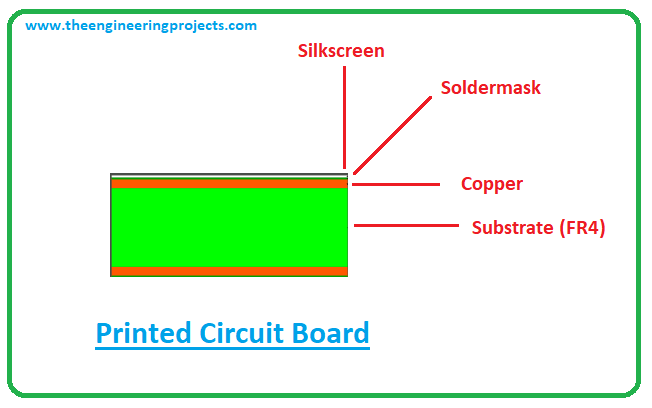
Solder mask is a thin, polymer-based protective layer applied to a Printed Circuit Board (PCB) to shield copper traces from oxidation and prevent unintended solder bridges during the assembly process. For Ball Grid Array (BGA) components, which utilize an array of tiny solder balls on their underside for electrical and mechanical connection, this solder mask layer assumes an even more pivotal role. The precise thickness of this layer directly influences the quality of the connection between the BGA solder balls and the PCB pads, affecting both mechanical stability and electrical performance.
In typical PCB manufacturing, solder mask thickness usually falls within the range of 0.8 to 1.2 mils (20 to 30 micrometers). However, in BGA applications, even minor deviations within this range can lead to critical issues such as inadequate solder joint formation or excessive interference from the mask. If the solder mask is excessively thick, it may impinge upon the pad area, thereby diminishing the effective contact surface for the solder ball. Conversely, if it is too thin, it might not provide sufficient protection, potentially resulting in short circuits or contamination during the intricate BGA assembly process.
Solder Mask Defined (SMD) vs. Non-Solder Mask Defined (NSMD) Pads: A Comparison
When designing pads for BGA components, a fundamental decision involves choosing between Solder Mask Defined (SMD) pads and Non-Solder Mask Defined (NSMD) pads. Each approach carries distinct implications for solder mask thickness and the ultimate reliability of the assembly.
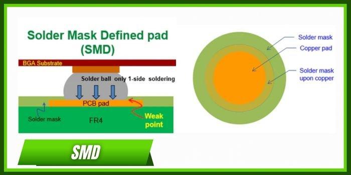
Solder Mask Defined (SMD) Pads
In the SMD pad configuration, the solder mask layer extends over the perimeter of the copper pad, effectively defining the precise area where solder is permitted to adhere. This method is often favored for finer pitch BGAs (where the center-to-center distance between solder balls is less than 0.5 mm) because it offers enhanced control over the solderable surface area. However, the solder mask thickness for BGA applications must be meticulously controlled with SMD pads. An overly thick mask can create a noticeable "step" or uneven surface that obstructs proper seating of the solder ball, leading to weakened joints. A recommended clearance of 2 to 3 mils (50 to 75 micrometers) between the solder mask opening edge and the copper pad edge is typically advised to circumvent such issues.
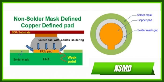
Non-Solder Mask Defined (NSMD) Pads
Conversely, NSMD pads are designed with the solder mask pulled back from the copper pad, leaving the entire pad surface, and sometimes a small portion of the surrounding trace, fully exposed. This design provides a larger solderable area, which generally contributes to stronger and more robust solder joints. For NSMD pads, the solder mask thickness is less of a direct concern regarding encroachment on the pad itself. Nonetheless, maintaining a consistent thickness—typically around 0.8 to 1.0 mils (20 to 25 micrometers)—is still crucial for ensuring proper electrical insulation and preventing unwanted solder bridging during the BGA assembly process.
For the majority of contemporary BGA designs, NSMD pads are preferred due to their demonstrated ability to form more reliable and mechanically stronger connections. Research indicates that NSMD pads can enhance solder joint reliability by up to 20% during thermal cycling tests when compared to SMD pads, particularly beneficial in high-density applications.
BGA Pad Design: Critical Factors for Optimal Connectivity
Beyond the choice between SMD and NSMD pads, comprehensive BGA pad design necessitates careful consideration of several interconnected factors to guarantee robust and reliable connections. These include the precise pad size, the pitch (spacing) of the solder balls, and how these elements integrate with the solder mask thickness specifically for BGA applications.
Pad Dimensions and Spacing
The optimal pad size for BGA components should typically be within 80-90% of the solder ball's diameter to facilitate proper wetting and fillet formation during reflow soldering. For instance, a 0.5 mm diameter solder ball would ideally be paired with a pad diameter ranging from 0.4 to 0.45 mm. The pitch, or the center-to-center spacing between solder balls, also significantly influences pad design. Fine-pitch BGAs (those with a pitch below 0.5 mm) often demand exceptionally tight control over solder mask thickness to prevent bridging, whereas components with larger pitches (0.8 mm and above) are generally more tolerant of slight variations.
Solder Mask Expansion
Solder mask expansion refers to the defined offset distance between the perimeter of the copper pad and the corresponding opening in the solder mask layer. For NSMD pads, a standard expansion of 2 to 4 mils (50 to 100 micrometers) is typically used. This expansion provides a necessary buffer for manufacturing tolerances and ensures that the entire copper pad remains exposed for soldering. Appropriate expansion also helps mitigate issues arising from misregistration during PCB fabrication, which could otherwise be catastrophic for BGA assembly if the solder mask encroaches upon the pad's solderable area.
Thermal Management and Electrical Performance
BGA pad design must also meticulously address thermal dissipation and signal integrity requirements. For high-power BGA components, incorporating thermal vias directly beneath the pads can significantly aid in heat removal. However, these vias must be properly tented or filled to prevent solder from wicking down into the hole. Furthermore, maintaining a consistent solder mask thickness contributes to precise impedance control in high-speed designs. A slightly thicker solder mask (e.g., around 1.2 mils or 30 micrometers) can subtly increase local capacitance, which, in certain scenarios, can be advantageous for mitigating noise in high-frequency signals operating above 1 GHz.
Solder Mask Thickness and the BGA Assembly Process
The BGA assembly process is a critical part of the PCB board assembly process, encompassing several key stages—from solder paste application and precise component placement to reflow soldering and post-reflow inspection. At each of these steps, the solder mask thickness for BGA components plays a subtle yet crucial role in ensuring reliable solder joint formation, minimizing defects, and achieving consistent assembly quality.
Solder Paste Deposition
During the solder paste printing phase, the solder mask effectively acts as a guide for the stencil, ensuring that solder paste is deposited only onto the intended pads. If the solder mask thickness is inconsistent or excessively thick (exceeding 1.5 mils or 38 micrometers), it can lead to non-uniform paste deposition, resulting in voids or insufficient solder volume for the BGA balls. A uniform thickness of 0.8 to 1.2 mils (20 to 30 micrometers) is considered ideal for maintaining precision during this crucial step.
Component Placement Accuracy
Accurate placement of the BGA component is paramount. The solder mask assists in this by providing visual references for alignment. For SMD pads, the mask's precisely defined edge delineates the pad boundary, meaning any variations in thickness or misregistration can potentially mislead automated component placement machinery. While NSMD pads offer more flexibility due to the fully exposed pad, the solder mask must still be consistent around the pad to prevent any interference with the component's proper seating.
Reflow Soldering Quality
In the reflow soldering stage, the BGA's solder balls melt and form metallurgical bonds with the PCB pads. A solder mask that is too thick can create a physical barrier, inhibiting proper wetting of the solder and leading to weak or incomplete joints. Conversely, a mask that is too thin might fail to contain the molten solder, allowing it to spread beyond the pad and potentially create shorts. Adhering to the recommended thickness range ensures the solder flows uniformly, forming reliable connections that typically achieve shear strength values exceeding 5 kg for standard 0.5 mm pitch BGAs.
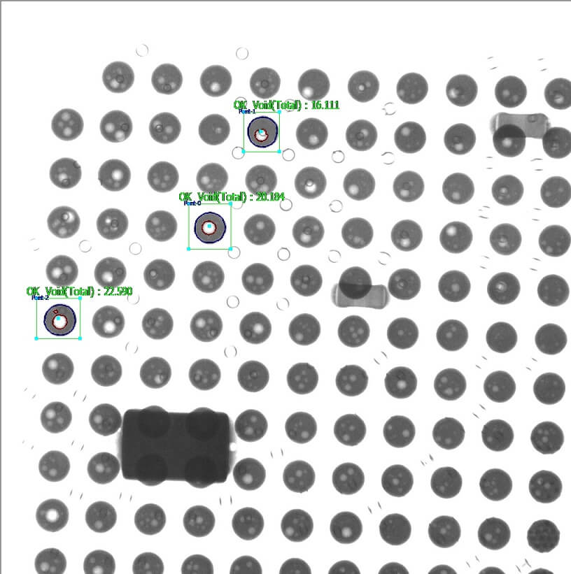
Post-Assembly Inspection and Testing
Following assembly, BGAs undergo rigorous inspection, often utilizing X-ray systems, to detect defects such as voids, misalignments, or insufficient solder joints. A well-controlled and consistent solder mask thickness significantly minimizes the occurrence of these defects, thereby reducing the necessity for costly rework. For instance, industry studies suggest that a solder mask thickness deviation of merely 0.2 mils (5 micrometers) can increase voiding rates by as much as 10%, underscoring the vital importance of precision in this aspect.
Best Practices for Managing Solder Mask Thickness in BGA Designs
To achieve consistently reliable connections in BGA assembly, integrating these actionable best practices for managing solder mask thickness and related design elements is essential.
Design Specification and Collaboration
● Specify Thickness in Fabrication Documents: Explicitly state the desired solder mask thickness (e.g., 0.8 to 1.2 mils or 20 to 30 micrometers) within your PCB design files and fabrication notes. This clear communication helps prevent manufacturing discrepancies.
● Prioritize NSMD for Most Applications: Unless specific fine-pitch constraints dictate otherwise, opt for Non-Solder Mask Defined (NSMD) pads to maximize the solderable area and enhance joint reliability.
● Control Solder Mask Expansion: For NSMD pads, set a solder mask expansion value typically ranging from 2 to 4 mils (50 to 100 micrometers) to accommodate standard fabrication tolerances and ensure full pad exposure.
● Engage with Fabricators: Establish close collaboration with your online PCB manufacturer. This partnership is crucial for ensuring consistent and high-quality application of the solder mask, particularly for intricate, high-density BGA layouts.
● Validate with Prototypes: Conduct comprehensive thermal cycling and mechanical stress tests on prototype boards. This validates that the chosen solder mask thickness and pad design can withstand the anticipated operational demands and environmental conditions.
Addressing and Overcoming Common Challenges
Despite meticulous planning, challenges related to solder mask thickness for BGA components can still emerge. Here are some prevalent issues and their corresponding solutions.
Solder Mask Misregistration
Misregistration occurs when the solder mask layer is not perfectly aligned with the underlying copper pads, potentially covering a portion of the intended solderable area. This issue is particularly problematic for SMD pads. To mitigate this, consider using a slightly larger solder mask expansion and specify tight registration tolerances (e.g., ±2 mils or ±50 micrometers) during the PCB fabrication process.
Prevention of Solder Bridging
For fine-pitch BGAs, the risk of solder bridging between adjacent pads is elevated if the solder mask is too thin or unevenly applied. To counteract this, ensure that the solder mask thickness is at least 0.8 mils (20 micrometers) and consider utilizing high-quality Liquid Photoimageable (LPI) solder mask materials, which offer superior resolution and definition.
Mitigating Thermal Stress Failures
During operational cycles, BGAs are subjected to repeated thermal expansion and contraction, which can induce significant mechanical stress on solder joints. A consistent solder mask thickness helps maintain the integrity of the pad structure, while NSMD designs inherently distribute stress more evenly across the entire solder joint. This even distribution can reduce failure rates by up to 15% in certain thermal cycling tests, thereby enhancing the long-term reliability of the assembly.
Conclusion: Precision in Solder Mask Thickness for BGA Success
In the demanding realm of high-density PCB design, every minute detail holds considerable weight, and the thickness of the solder mask for BGA assembly is certainly no exception. By meticulously managing this critical parameter, in conjunction with a well-thought-out BGA pad design utilizing either Solder Mask Defined (SMD) or Non-Solder Mask Defined (NSMD) pads, engineers can ensure the formation of highly reliable connections throughout the entire BGA assembly process. Whether you are working with extremely fine-pitch components or high-power applications, adhering to established best practices for solder mask thickness—typically within the range of 0.8 to 1.2 mils (20 to 30 micrometers)—and fostering close collaboration with your PCB manufacturer will invariably lead to superior outcomes. With this precise and informed approach, you can effectively minimize manufacturing defects, significantly enhance overall performance, and ultimately construct PCBs that exhibit remarkable endurance and reliability over time.


