Introduction
In high-speed PCB designs, maintaining signal integrity has become increasingly challenging as clock rates exceed several gigahertz and data throughput demands rise. Common issues like electromagnetic interference, crosstalk, and high-frequency noise can degrade signal quality, leading to bit errors, timing violations, and system failures. Ferrite bead filters offer a proven method for signal integrity improvement PCB by targeting unwanted high-frequency components while preserving low-frequency signals and DC power delivery. These passive components provide high impedance at RF frequencies, effectively suppressing noise without significantly impacting the desired signal bandwidth. Engineers must integrate ferrite beads thoughtfully into layouts to achieve optimal performance, especially in multilayer boards with dense routing. This guide explores the principles, placement strategies, and best practices for using ferrite beads in PCB design ferrite beads applications.
What Are Ferrite Bead Filters and Why Do They Matter for Signal Integrity?
Ferrite bead filters are surface-mount or through-hole components made from ferrite material, typically consisting of a magnetic core with conductive windings or a solid bead structure. At low frequencies and DC, they exhibit very low resistance, allowing signals to pass unimpeded, but their impedance rises sharply above a cutoff frequency due to magnetic hysteresis and eddy current losses. This frequency-dependent behavior makes them ideal for high-frequency noise suppression PCB, where they act as lossy inductors rather than traditional low-loss coils. In PCB contexts, ferrite beads address common signal integrity problems arising from switching regulators, clock harmonics, and external EMI coupling into traces.
The relevance of ferrite beads intensifies in modern electronics, where shrinking geometries and faster edge rates amplify noise coupling. Without proper suppression, high-frequency components can propagate through power distribution networks, causing voltage ripples that affect sensitive analog or digital circuits. By deploying ferrite beads strategically, designers enhance signal integrity improvement PCB, ensuring compliance with performance margins in high-speed interfaces like USB, PCIe, or DDR memory buses. Their compact size and low cost further make them indispensable for both prototyping and production boards. Ultimately, ferrite beads bridge the gap between basic decoupling and advanced filtering, providing a simple yet effective layer of protection.
Technical Principles of Ferrite Beads in Signal Integrity
Ferrite beads operate on the principle of frequency-selective impedance, where the real part of impedance dominates at high frequencies due to material losses. Below the self-resonant frequency, they behave primarily as inductors with values ranging from nanoHenries to microHenries, but above it, parasitic capacitance and resistive losses take over, converting them into broadband attenuators. This characteristic enables ferrite bead filter impedance matching in noisy environments, where the bead's impedance can be tuned to match source or load conditions at problematic frequencies, minimizing reflections and standing waves. Engineers select beads based on impedance curves provided in datasheets, targeting peaks that align with noise spectra, typically from 10 MHz to several GHz.
High-frequency noise suppression PCB relies on the bead's ability to dissipate energy as heat through magnetic domain movements and eddy currents in the ferrite core. Unlike capacitors, which shunt noise to ground, ferrite beads isolate noise in series, preventing its propagation along traces or planes. In power delivery networks, this isolation reduces simultaneous switching noise from ICs, stabilizing voltage rails. According to IPC-2251 guidelines for high-speed PCB design, incorporating such components helps mitigate EMI-related signal degradation in controlled impedance environments. The interaction with PCB parasitics, like via inductance and trace capacitance, must also be considered to avoid unintended resonances that could amplify noise.
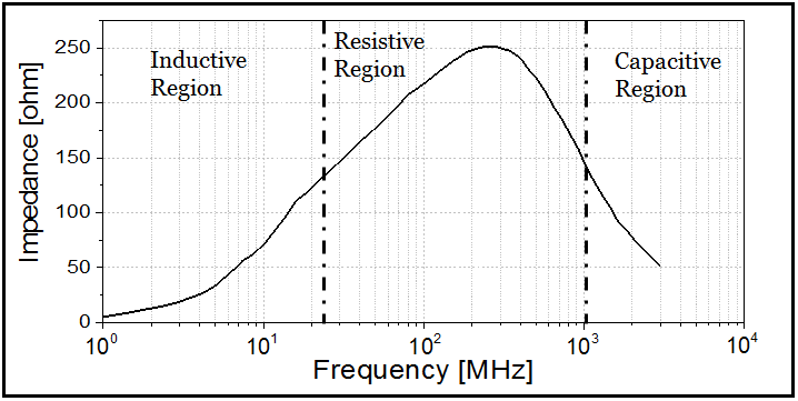
Material composition plays a critical role, with nickel-zinc ferrites suited for frequencies up to 100 MHz and manganese-zinc for higher bands. Current ratings limit bead selection, as saturation reduces effectiveness under high DC bias. Simulations reveal that beads in pi-configurations with bypass capacitors form second-order filters, achieving greater than 20 dB attenuation at targeted harmonics. These principles ensure ferrite beads contribute reliably to overall signal integrity without introducing new distortions.
Ferrite Bead Placement Strategies in PCB Design
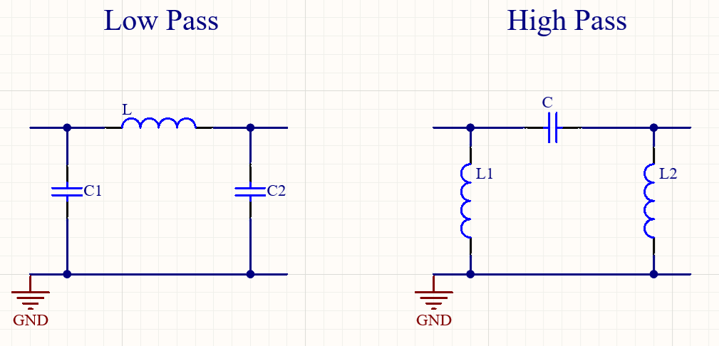
Effective ferrite bead placement strategies begin with proximity to the noise source, such as directly at IC power pins or regulator outputs, to attenuate interference before it spreads. On power rails, position beads between bulk decoupling capacitors and local bypass caps to form a pi-filter topology, which presents high impedance to noise while maintaining low impedance to DC. For I/O lines, beads suppress common-mode noise on differential pairs, but avoid series placement on high-speed data signals unless ringing analysis justifies it, as added inductance can slow rise times. Ground return paths must remain short and wide to maximize filter efficacy.
In multilayer PCBs, layer stacking influences placement; beads on inner power planes require via optimization to minimize stub inductance. High-frequency noise suppression PCB benefits from symmetric routing around beads, ensuring balanced current flow and reduced loop areas. According to IPC-2221 standards for printed board design, component orientation should align with current direction to prevent asymmetric fields that exacerbate EMI. Testing with network analyzers validates placement by measuring insertion loss and return loss across frequencies.
Consider thermal dissipation, as high-impedance operation generates heat; space beads away from heat-sensitive components. Multi-bead cascades target broader spectra, with each bead optimized for different frequency bands. These strategies, when combined with ground plane partitioning, yield robust signal integrity improvement PCB.
Best Practices for Implementing Ferrite Beads in PCB Design
Selection starts with impedance profiling against expected noise, prioritizing beads with rated currents exceeding peak loads to avoid droop. Integrate beads early in schematic capture, modeling them with equivalent R-L-C circuits for pre-layout simulations. During routing, allocate dedicated vias for bead connections, keeping stub lengths under 1/10th wavelength at the highest frequency of interest. Ferrite bead placement strategies extend to shielding; enclose noisy sections with ground pours tied to multiple vias.
Fabrication considerations include solder joint reliability per J-STD-001 requirements for soldered assemblies, ensuring beads withstand reflow profiles without cracking. Post-layout verification involves S-parameter extraction to confirm ferrite bead filter impedance matching, adjusting values iteratively if resonances appear. Decouple beads with 0.1 μF ceramics within 2 mm to enhance filtering. Avoid paralleling beads randomly, as mismatched impedances can degrade performance.
Documentation in Gerber files should highlight bead locations for assembly teams. Field testing with spectrum analyzers quantifies suppression, guiding refinements. These practices ensure ferrite beads deliver consistent high-frequency noise suppression PCB across prototypes and volumes.
Troubleshooting Common Signal Integrity Issues with Ferrite Beads
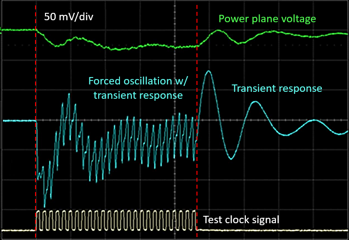
Over-placement of ferrite beads can introduce excessive series inductance, slowing signal edges and violating timing budgets in high-speed links. Diagnose by scoping eye diagrams; if closure occurs, remove or replace with lower-inductance options. Saturation from underrated current handling manifests as voltage sag under load, measurable with dynamic load tests. Resonance between bead capacitance and PCB inductance peaks noise; mitigate by adding shunt capacitors or selecting higher-SRF beads.
Improper grounding loops amplify common-mode noise despite beads; verify continuous ground planes with 2D field solvers. If EMI persists post-implementation, sweep impedance to identify untargeted bands and cascade beads accordingly. Thermal imaging reveals hot spots indicating overload. Systematic troubleshooting preserves the intended signal integrity improvement PCB.
Conclusion
Ferrite bead filters stand as essential tools for optimizing PCB signal integrity, offering targeted high-frequency noise suppression through strategic impedance control. Key to success lies in understanding their frequency-dependent behavior, precise placement near sources, and integration with decoupling schemes. Adhering to standards like IPC-2251 and IPC-2221 ensures designs meet performance and reliability thresholds. By applying these principles, engineers achieve cleaner signals, reduced EMI, and robust system operation. Future designs will increasingly rely on such passive solutions amid rising speeds, underscoring the need for ongoing expertise in PCB design ferrite beads.
FAQs
Q1: What role does ferrite bead filter impedance matching play in PCB design?
A1: Ferrite bead filter impedance matching aligns the bead's frequency-dependent impedance with noise characteristics, maximizing attenuation while minimizing signal distortion. Placed in series, it absorbs high-frequency energy through losses, preventing propagation. This technique suits power lines and I/O, enhancing overall stability without complex active circuits. Proper selection via impedance plots ensures optimal performance across operating bands.
Q2: How can ferrite bead placement strategies improve signal integrity in PCBs?
A2: Ferrite bead placement strategies focus on proximity to noise sources, forming pi-filters with capacitors for superior rejection. Close IC mounting and short vias reduce loop inductance, bolstering effectiveness. Avoid data lines unless needed to prevent edge slowing. These approaches yield measurable signal integrity improvement PCB, as validated by time-domain reflectometry.
Q3: Why are ferrite beads essential for high-frequency noise suppression PCB?
A3: Ferrite beads excel at high-frequency noise suppression PCB due to rising impedance from magnetic losses, shunting RF while passing DC. They isolate switching noise in PDNs, stabilizing rails for sensitive loads. Unlike capacitors, they break conduction paths, complementing ground strategies. Implementation per design guidelines prevents EMI compliance failures.
Q4: What are common mistakes in PCB design ferrite beads integration?
A4: Common pitfalls include current underrating causing saturation, distant placement allowing noise spread, and ignoring resonances with PCB parasitics. Overuse on signals adds unwanted inductance. Mitigate through simulation, thermal checks, and standards like J-STD-001 for assembly. Corrected designs achieve reliable signal integrity.
References
IPC-2251 — High-Speed/High-Frequency Design and Manufacturing Standard. IPC.
IPC-2221B — Generic Standard on Printed Board Design. IPC, 2012.
J-STD-001G — Requirements for Soldered Electrical and Electronic Assemblies. IPC/JEDEC, 2011.


