Why Is Design for Assembly (DFA) Crucial for Engineers?
Design for Assembly (DFA) is a systematic approach focused on simplifying a product's assembly process during its initial design stages. For engineers, adopting DFA means proactively addressing potential manufacturing hurdles, thereby reducing the time and resources typically spent on rectifying issues once production begins. This forward-thinking methodology leads to fewer errors, decreases labor expenses, and ultimately accelerates a product's journey to market.

Evidence suggests that over 70% of a product's final cost is determined during its design phase. This makes DFA an indispensable tool for effective cost management across various engineering disciplines, from consumer electronics to industrial machinery. By adhering to DFA principles, engineers ensure their designs are inherently easier to assemble and more robust in real-world applications.
What Are the Key Principles of a DFA Checklist for Engineers?
Reducing the Number of Components
A fundamental tenet of DFA is to minimize the total part count in a design. Fewer parts translate directly to fewer assembly steps, lower inventory holding costs, and a reduced likelihood of manufacturing defects. Engineers should critically evaluate each component, asking if its function can be integrated into another part or if it is truly indispensable. For instance, combining a bracket and a housing into a single molded piece can eliminate an assembly operation and potentially cut material costs.
Functional analysis, often guided by established DFA frameworks like Boothroyd Dewhurst, helps identify redundant elements. Such analyses determine if a component moves relative to others, requires a unique material, or serves an exclusive purpose that cannot be merged. In electronics, consolidating multiple discrete resistors into a single resistor array can notably decrease placement time during automated surface-mount technology (SMT) assembly.
Embracing Standardized Parts
Opting for standardized components significantly simplifies procurement, lowers costs, and enhances overall product reliability. Custom-made parts frequently necessitate specialized tooling, which can substantially inflate production expenses. In contrast, standard components—like common fasteners or widely available integrated circuits—are readily accessible, typically more affordable, and already proven in terms of reliability.
For printed circuit boards (PCBs), using industry-standard components such as 0805 resistors or SOIC packages ensures compatibility with automated pick-and-place machinery. Choosing a standard fastener, like an M3 screw, over a custom alternative can shave precious seconds off assembly time per unit in high-volume production scenarios.
Designing for Self-Alignment and Integrated Fastening
Parts designed to be self-locating automatically guide themselves into the correct position during assembly, thereby reducing the need for jigs, fixtures, or painstaking manual alignment. Similarly, self-fastening features, such as snap-fits or press-fits, eliminate the need for separate fasteners like screws or adhesives, which can dramatically reduce assembly time.
Incorporating design elements such as chamfers, tabs, or slots helps parts align intuitively. For PCBs, clear "pin 1" markings are essential to prevent incorrect component orientation during assembly. A consumer device featuring a snap-fit enclosure, for example, can see a significant reduction in assembly time compared to one that relies on multiple screws.
Optimizing Component Layout
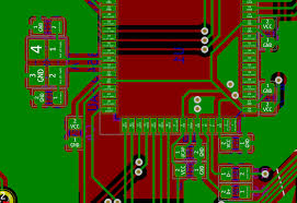
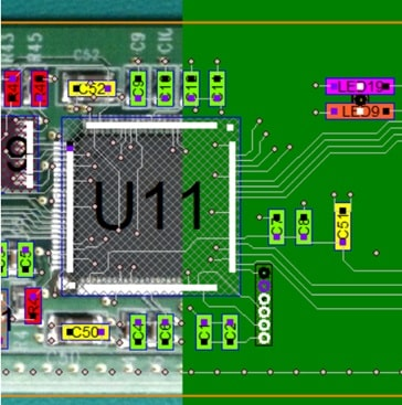
Strategic placement of components, whether on a PCB or within a mechanical assembly, is vital for minimizing errors and improving thermal performance. On types of PCBs, it's advisable to maintain specific clearances—for instance, components should be placed at least 7 mil from annular rings and 8 mil from holes to prevent issues like solder mask bridges or misalignment during fabrication.
Grouping components by their function (e.g., power circuits, signal paths, or control logic) can reduce signal interference and simplify subsequent soldering processes. Utilizing automated placement tools further assists in creating efficient and error-free layouts. Thoughtful placement, such as positioning high-heat components away from sensitive integrated circuits, can significantly reduce thermal stress and enhance long-term reliability.
Streamlining Assembly Procedures
Complicated assembly steps are direct contributors to increased labor costs and higher error rates. Products should be designed to minimize the number of unique tools or distinct operations required. For example, reducing the variety of fasteners used in an assembly can lead to a considerable decrease in overall assembly time.
Adopting modular design principles allows complex products to be broken down into smaller, independently buildable and testable subassemblies. For PCBs, ensuring that component footprints precisely match datasheet specifications is crucial to avoid costly rework during manufacturing. A modular PCB design featuring pre-assembled daughterboards can substantially cut down final assembly time compared to a monolithic, complex board.
Integrating Poka-Yoke (Mistake-Proofing)
Poka-yoke, or mistake-proofing, involves designing parts in such a way that assembly errors are prevented by default. This could include asymmetrical features or uniquely shaped connectors that ensure components can only be installed in the correct orientation.
On PCBs, incorporating polarized connectors or keyed slots effectively eliminates orientation mistakes. It is also critical to verify that polarity markings are clearly indicated in all assembly documentation. For instance, a keyed USB-C connector inherently prevents incorrect insertion, thereby reducing assembly errors compared to non-polarized alternatives.
Specifying Appropriate Tolerances
While precision is important, excessively tight tolerances can dramatically increase manufacturing costs without always yielding a proportional improvement in performance. For PCBs, specifying tolerances below 5 mil should be avoided unless absolutely necessary, as tighter specifications can significantly drive up fabrication expenses.
Engineers should review the manufacturing equipment's process capabilities and specify tolerances that fall within those practical limits. For mechanical parts, incorporating features like chamfers or fillets can help accommodate minor misalignments. A 7 mil clearance for component-to-hole spacing on a PCB, for example, is generally compatible with standard SMT processes, helping to prevent expensive rework.
Ensuring Accuracy of Footprints and Bills of Material
Inaccuracies in component footprints or the Bill of Materials (BOM) can bring production to a grinding halt. A common error, such as a footprint designed for an 0806 resistor when the BOM specifies an 0402, can lead to significant assembly delays and additional costs.
It is imperative to meticulously cross-check all footprints against component datasheets and verify every detail in the BOM, including manufacturer part numbers (MPNs) and quantities. Leveraging automated DFA software to validate footprints can effectively reduce errors, ensuring a seamless transition from the design phase to assembly.
Facilitating Testing and Inspection
Product designs should inherently include features that simplify subsequent testing and inspection processes. This means incorporating elements such as dedicated test points or easily accessible solder joints. These considerations reduce the time required for quality control and contribute to improved yield rates.
On PCBs, adding test points for critical nets, like power and ground, and ensuring solder joints are clearly visible for automated optical inspection (AOI) are crucial. Maintaining appropriate solder mask clearances also helps prevent short circuits. Including these test points can notably reduce the time spent on board testing, thereby enhancing production throughput.
How Can Engineers Integrate DFA Principles into Their Workflow?
To effectively embed DFA into their design process, engineers should follow a structured approach. Begin with a baseline analysis, thoroughly documenting the existing assembly process, including time studies and defect rates, to establish clear benchmarks. Next, foster cross-functional collaboration by involving design, manufacturing, and quality assurance engineers early on to proactively identify and address assembly challenges.
Conducting a product teardown of prototypes allows teams to pinpoint specific steps that are time-consuming or prone to errors. Applying established DFA metrics, often with specialized software, helps quantify assembly efficiency and guides improvement efforts. Finally, an iterative design process, followed by validation through prototyping, confirms the anticipated cost and time savings. A notable example from the automotive industry demonstrated that applying DFA reduced assembly time by 40% and cut production costs by 30% for a dashboard module.
How Does AIVON Support DFA Implementation for Engineers?
At AIVON, we recognize the critical role DFA plays in achieving both cost-effective and reliable product designs. Our rapid prototyping services empower engineers to quickly test and refine their DFA-optimized designs, ensuring any potential issues are caught and addressed early in the development cycle. With robust global logistics and advanced manufacturing capabilities, we deliver high-quality PCB assembly solutions that align seamlessly with DFA principles, emphasizing precise component placement and standardized processes.
Furthermore, our team of experts offers comprehensive DFA reviews as an integral part of our turnkey PCB assembly service. This specialized support helps engineers identify key opportunities to simplify designs and reduce the PCB manufacturing cost, all without ever compromising on the crucial aspect of product quality.