Introduction
In the realm of PCB prototyping and assembly, achieving high quality remains a cornerstone for reliable electronic products. Automated Optical Inspection (AOI) stands as a pivotal technology in this process, enabling manufacturers to detect PCB defects with precision during surface mount technology (SMT) inspection. For electric engineers, understanding how AOI testing integrates into the PCB manufacturing workflow is essential. This article explores the significance of automated inspection in quality control, delving into its technical principles and practical applications. By leveraging AOI, prototyping assembly becomes more efficient, reducing errors and ensuring compliance with industry standards. Join us as we uncover the mechanisms behind AOI and its role in maintaining excellence in PCB production, tailored for professionals seeking actionable insights into the inspection process.
What Is Automated Optical Inspection (AOI) and Why It Matters
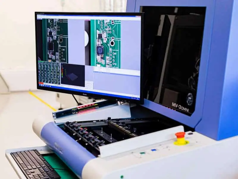
Automated Optical Inspection, commonly known as AOI, is a non-contact visual inspection method used in PCB manufacturing to identify defects during various stages of production. This technology employs high-resolution cameras, sophisticated lighting, and advanced image processing algorithms to scan printed circuit boards for issues such as misaligned components, solder defects, and missing parts. For electric engineers, AOI testing is critical because it ensures that proto PCB boards meet design specifications before moving to mass production.
The importance of AOI in quality control cannot be overstated. In SMT inspection, where components are densely packed, manual inspection becomes impractical due to human error and time constraints. AOI systems provide consistent, repeatable results, catching PCB defects early in the manufacturing cycle. This reduces rework costs and prevents faulty boards from reaching end users, safeguarding product reliability in applications ranging from consumer electronics to medical devices.
Technical Principles of AOI in PCB Inspection
The operation of AOI systems relies on a combination of hardware and software to achieve accurate defect detection. At its core, an AOI setup includes multiple high-resolution cameras positioned to capture detailed images of the PCB surface. These cameras work under controlled lighting conditions, often using different angles and wavelengths to highlight specific features or anomalies.
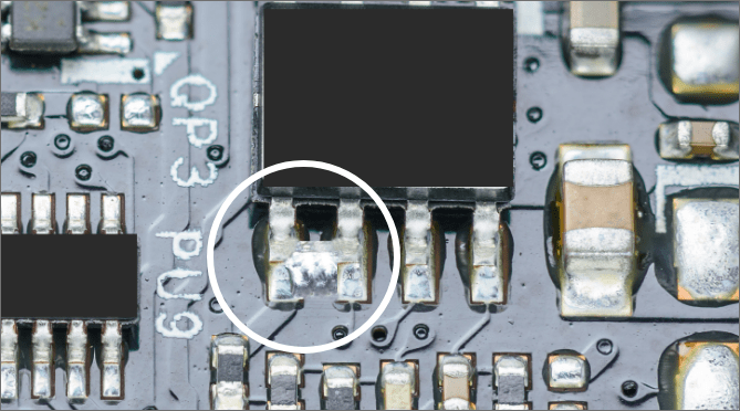
Once images are captured, sophisticated algorithms analyze them against a reference model or design data, such as Gerber files or CAD layouts. The software identifies deviations by comparing the scanned board to the ideal layout, flagging issues like component misalignment, insufficient solder, or bridged connections. Common defect categories in SMT inspection include tombstoning, where components stand upright, and cold solder joints, which compromise electrical connectivity.
AOI systems typically operate in two modes: 2D and 3D inspection. While 2D AOI focuses on surface-level defects, 3D systems measure height and volume, offering deeper insights into solder joint quality. This dual approach enhances the inspection process, ensuring comprehensive quality control across diverse PCB designs.
Types of PCB Defects Detected by AOI Testing
AOI testing excels at identifying a wide array of PCB defects that could impact functionality. Understanding these issues helps electric engineers prioritize inspection focus during prototyping assembly. Below are key defect types detected through automated inspection:
- Component Issues: Misplacement, rotation errors, or missing components on the board.
- Solder Defects: Insufficient solder, excess solder, or bridging between pads.
- Polarity Errors: Incorrect orientation of polarized components like diodes or capacitors.
- Surface Anomalies: Scratches, contamination, or damaged traces on the PCB surface.
- Billboarding and Tombstoning: Components lifted on one side or standing vertically due to uneven soldering.
By addressing these defects early, AOI ensures that the PCB manufacturing process aligns with stringent quality standards, minimizing the risk of failures in critical applications.
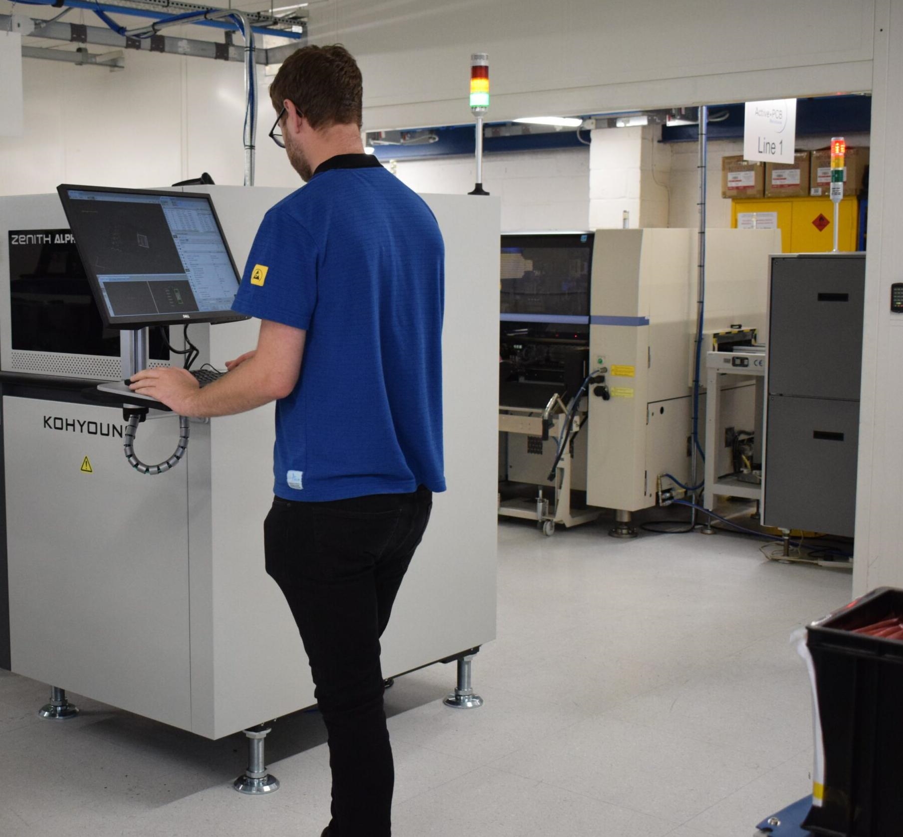
Practical Applications of AOI in PCB Prototyping Assembly
In PCB prototyping assembly, AOI plays a vital role across multiple production stages. During pre-reflow inspection, AOI verifies component placement accuracy after pick-and-place operations in SMT PCB assembly. This step prevents misalignments from becoming permanent after soldering. Post-reflow inspection, another critical phase, examines solder joint quality to confirm proper bonding and detect defects like cold joints.
For electric engineers working on prototypes, AOI offers immediate feedback, allowing rapid design iterations. If a defect is detected, the system generates detailed reports pinpointing the issue, enabling quick corrective actions. This capability is especially valuable in high-mix, low-volume production, where frequent design changes are common. Moreover, AOI integrates seamlessly with other quality control measures, such as solder paste inspection, to form a robust inspection process.
Beyond defect detection, AOI contributes to process optimization. By analyzing defect trends, engineers can identify recurring issues, such as specific component types prone to misalignment, and adjust assembly parameters accordingly. This data-driven approach enhances overall manufacturing efficiency.
Best Practices for Implementing AOI in Quality Control
To maximize the benefits of AOI testing in PCB manufacturing, electric engineers should adhere to several best practices. First, ensure that the AOI system is calibrated regularly to maintain accuracy. Calibration involves updating reference data and adjusting camera settings to match the specific board design being inspected.
Second, define clear defect criteria based on industry standards. For instance, acceptability criteria for solder joints can be aligned with guidelines from widely recognized specifications. This ensures consistency in defect classification and reduces false positives, where acceptable variations are flagged as errors.
Third, position AOI strategically within the production line. Conducting inspections immediately after critical steps like component placement and reflow soldering allows for early defect detection. Additionally, train personnel to interpret AOI reports effectively, focusing on actionable insights rather than raw data. Combining human expertise with automated inspection creates a balanced quality control framework.
Finally, maintain a defect library within the AOI system. This database stores images and descriptions of past defects, improving the software’s ability to recognize similar issues in future inspections. Such proactive measures strengthen the reliability of SMT inspection over time.
Challenges in AOI Implementation and Solutions
While AOI offers significant advantages, certain challenges can arise during its implementation in PCB prototyping assembly. One common issue is the occurrence of false positives, where the system flags non-defective features as errors. This often happens due to variations in board finishes or component markings. To address this, engineers can refine the inspection algorithms by updating the reference model with real-world data.
Another challenge is the limitation of AOI in detecting internal defects, such as voids within solder joints. Since AOI focuses on surface-level inspection, it must be complemented with other methods like X-ray inspection for a complete quality assessment. Integrating multiple inspection technologies ensures comprehensive coverage of PCB defects.
Lastly, the initial setup cost and learning curve for AOI systems can be substantial. To mitigate this, start with pilot projects on smaller production runs to gain familiarity with the technology. Over time, the reduction in rework and improved yield will offset the investment, making AOI a cornerstone of modern quality control.
Conclusion
Automated Optical Inspection stands as an indispensable tool in PCB prototyping assembly, delivering unmatched precision in detecting PCB defects and ensuring quality control. For electric engineers, mastering AOI testing within the SMT inspection framework translates to fewer errors, faster iterations, and reliable prototypes. By understanding its technical principles and applying best practices, professionals can optimize the inspection process to meet stringent industry standards. As PCB designs grow more complex, integrating AOI into manufacturing workflows will remain essential for maintaining excellence. This technology not only enhances product reliability but also streamlines production, paving the way for innovation in electronic applications.
FAQs
Q1: How does AOI testing improve quality control in PCB manufacturing?
A1: AOI testing enhances quality control by providing fast, accurate detection of PCB defects like misaligned components and solder issues. It reduces human error during SMT inspection, ensuring consistent results. By catching problems early, AOI minimizes rework costs and prevents faulty boards from reaching end users, aligning production with industry standards for reliability.
Q2: What types of PCB defects can automated inspection identify?
A2: Automated inspection excels at spotting various PCB defects, including component misalignment, missing parts, solder bridging, and polarity errors. It also detects surface issues like scratches or contamination. During the inspection process, AOI ensures these defects are flagged before they impact the functionality of the final product.
Q3: Why is SMT inspection critical in PCB prototyping assembly?
A3: SMT inspection is vital in PCB prototyping assembly because surface mount components are small and densely packed, making manual checks prone to errors. AOI systems provide precise evaluation of placement and soldering, ensuring quality control. This step is crucial for validating designs before scaling to mass production.
Q4: How can engineers optimize the AOI inspection process for better results?
A4: Engineers can optimize the AOI inspection process by calibrating systems regularly, defining clear defect criteria based on standards, and maintaining a defect library. Positioning AOI at key production stages like post-placement and reflow also helps. Combining human expertise with automated data analysis further improves accuracy in detecting PCB defects.
References
IPC-A-600K — Acceptability of Printed Boards. IPC, 2020.
IPC-6012E — Qualification and Performance Specification for Rigid Printed Boards. IPC, 2020.
IPC J-STD-001H — Requirements for Soldered Electrical and Electronic Assemblies. IPC, 2020.
ISO 9001:2015 — Quality Management Systems. ISO, 2015.


