Introduction
Printed Circuit Board (PCB) design involves balancing performance, functionality, and cost. One often overlooked factor is PCB size optimization, which directly influences component costs and overall project expenses. Board dimensions affect material usage, manufacturing efficiency, and assembly complexity, making size a critical consideration for electrical engineers. By focusing on minimizing board area and optimizing PCB shape for cost, designers can achieve significant savings without compromising quality. This article explores how PCB size impacts expenses, delves into panelization cost savings, and provides actionable strategies to streamline designs. Aimed at engineers and technical professionals, the content aligns with industry standards to ensure reliable and practical insights for optimizing designs in real-world applications.
Why PCB Size Matters in Cost Management
PCB size plays a pivotal role in determining the overall cost of a project. Larger boards require more raw materials, such as copper-clad laminates and substrates, which increase expenses before manufacturing even begins. Additionally, bigger dimensions often lead to higher fabrication costs due to increased processing time and equipment wear. Assembly costs also rise with size, as more space can complicate component placement and soldering processes. Beyond direct costs, oversized boards may lead to inefficiencies in panelization, where multiple PCBs are arranged on a single manufacturing panel. Poor panel utilization results in wasted material and reduced cost savings. For engineers, understanding the relationship between PCB cost and size is essential to delivering efficient, budget-friendly designs that meet performance requirements.
Technical Principles Behind PCB Size and Cost Relationships
Material Usage and Board Dimensions
The most direct link between PCB size and cost lies in material consumption. Larger boards use more base materials, such as FR-4 or other substrates, which are priced per square unit. Even a small increase in dimensions can significantly raise material expenses, especially for high-volume production. Copper layers, solder masks, and silkscreen also scale with board area, compounding costs. Engineers must evaluate whether additional space is necessary for component placement or if tighter layouts can achieve the same functionality with reduced material use.
Manufacturing Constraints and Panelization
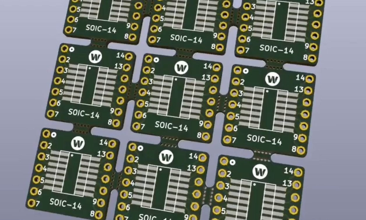
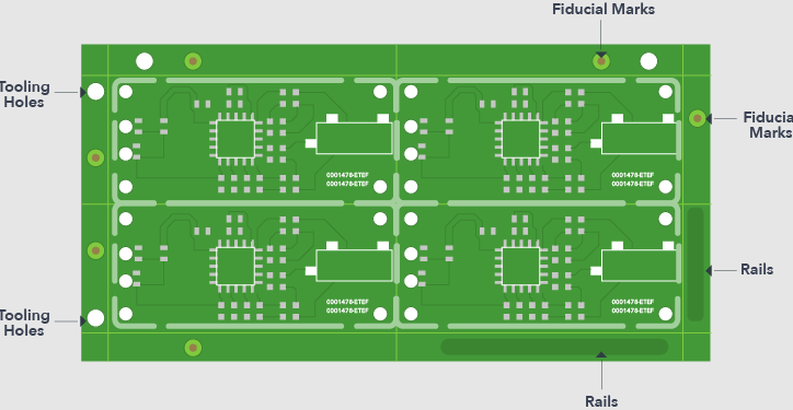
Panelization refers to arranging multiple PCBs on a single manufacturing panel to maximize efficiency. Standard panel sizes vary, often around 18 by 24 inches, though exact dimensions depend on fabrication capabilities. When PCB designs do not fit efficiently within these panels, material waste increases, reducing panelization cost savings. For instance, irregular shapes or oversized boards may leave unused panel space, driving up costs per unit. Fabrication houses often charge based on panel usage, so optimizing PCB shape for cost through efficient nesting is crucial.
Assembly and Component Placement Challenges
Larger PCBs can complicate assembly processes. More surface area often means longer traces, increasing the risk of signal integrity issues and requiring additional design considerations. Assembly equipment may need recalibration for bigger boards, adding setup time and labor costs. Component placement also becomes less efficient if parts are spread out, potentially requiring multiple passes through pick-and-place machines. These factors elevate assembly expenses, making minimizing board area a priority for cost-conscious engineers.
Testing and Quality Control Overhead
Testing larger PCBs often demands more time and resources. Probe fixtures for in-circuit testing must cover greater areas, increasing fixture costs. Thermal and electrical testing may reveal issues tied to extended traces or uneven heat distribution on oversized boards. These challenges can lead to higher rejection rates or rework, further impacting budgets. By focusing on PCB size optimization, engineers can streamline testing processes and reduce quality control overhead.
Suggested Reading: The Maximum PCB Size Sweet Spot for Cost Effective Prototyping
Practical Strategies for Minimizing Board Area
Component Layout Optimization
Efficient component placement is the foundation of minimizing board area. Group related components together to shorten trace lengths and reduce the overall footprint. Use both sides of the board when possible to maximize space without increasing dimensions. Prioritize high-density layouts, ensuring clearance and creepage distances comply with standards like IPC-2221B for voltage spacing requirements. This approach not only cuts material costs but also improves signal performance.
Layer Stackup Considerations
Increasing the number of layers can reduce board size by allowing denser routing in a smaller area. While multilayer boards may have higher per-unit fabrication costs, the savings from reduced dimensions often outweigh this expense in high-volume runs. Balance layer count with cost by analyzing signal and power requirements early in the design phase. Standards such as IPC-6012E provide guidance on layer stackup quality and performance to ensure reliability.
Shape Optimization for Panelization
Optimizing PCB shape for cost involves designing boards to fit neatly within standard panel sizes. Rectangular or square shapes typically nest better than irregular outlines, maximizing panel utilization. Avoid unnecessary cutouts or protrusions that waste space during panelization. Work with fabrication partners to understand panel constraints and design for efficient layouts, achieving panelization cost savings. Tools aligned with industry practices can simulate panel arrangements before production.
Design for Manufacturability
Incorporate design for manufacturability (DFM) principles to align PCB dimensions with fabrication capabilities. Adhere to minimum trace widths, spacing, and drill sizes as outlined in standards like IPC-A-600K for acceptability of printed boards. Smaller boards with standardized features reduce setup times and minimize errors during production. Early DFM reviews can identify size-related cost drivers, allowing adjustments before manufacturing begins.
Balancing Size Reduction with Performance
While minimizing board area offers clear cost benefits, engineers must ensure performance remains uncompromised. Overly compact designs can lead to thermal management issues, as components packed too closely may overheat. Signal integrity can suffer if traces are shortened excessively or routed improperly. Standards like IPC-2221B provide guidelines for spacing and layout to prevent such problems. Evaluate power distribution needs and grounding strategies to avoid noise in dense layouts. Simulation tools can predict performance impacts of size reductions, helping strike a balance between cost and functionality.
Insights on Cost Impacts in Real-World Designs
Consider a scenario where a design team reduces a PCB's dimensions by 20 percent through layout optimization. Material costs drop proportionally, and panelization efficiency improves, fitting more units per panel. Assembly time decreases due to a smaller area, lowering labor expenses. However, the team must verify that component density does not violate clearance rules or cause thermal stress, referencing standards like JEDEC J-STD-020E for moisture and reflow sensitivity. Such real-world adjustments demonstrate how PCB size and cost are intertwined, with careful planning yielding measurable savings.
Conclusion
PCB size optimization is a powerful strategy for managing component costs and overall project budgets. Board dimensions influence material usage, manufacturing efficiency, assembly complexity, and testing overhead, making size a critical design factor. By focusing on minimizing board area and optimizing PCB shape for cost, engineers can achieve significant savings through efficient panelization and streamlined processes. Adhering to industry standards ensures that size reductions do not compromise reliability or performance. With thoughtful design practices, electrical engineers can deliver cost-effective solutions that meet both technical and financial goals in competitive markets.
FAQs
Q1: How does PCB size impact overall project costs?
A1: PCB size directly affects material, manufacturing, and assembly expenses. Larger boards use more raw materials and may lead to inefficient panelization, reducing cost savings. Assembly and testing also become costlier with increased dimensions. By focusing on PCB size and cost optimization, engineers can lower expenses while maintaining quality, using efficient layouts and panel-friendly designs as guided by industry standards.
Q2: What are the benefits of minimizing board area in PCB design?
A2: Minimizing board area reduces material usage, cuts fabrication costs, and improves panelization efficiency. It also shortens assembly time and simplifies testing, lowering labor expenses. Smaller boards can enhance signal integrity if designed properly. Following standards like IPC-2221B ensures that reduced size does not affect performance, making this approach a key strategy for cost-effective design.
Q3: How can panelization lead to cost savings in PCB production?
A3: Panelization cost savings occur when multiple PCBs are arranged efficiently on a single manufacturing panel. Optimal nesting reduces material waste and maximizes output per panel, lowering per-unit costs. Designing boards with standard shapes and sizes enhances panel utilization. Engineers can achieve significant savings by aligning designs with fabrication panel constraints during the planning phase.
Q4: What role does optimizing PCB shape play in reducing expenses?
A4: Optimizing PCB shape for cost ensures better fit within manufacturing panels, minimizing wasted space. Rectangular or square designs typically nest more efficiently than irregular shapes, reducing material costs. Efficient shapes also streamline fabrication and assembly processes. By prioritizing shape optimization, engineers can lower expenses while adhering to industry guidelines for manufacturability and performance.
References
IPC-2221B — Generic Standard on Printed Board Design. IPC, 2012.
IPC-6012E — Qualification and Performance Specification for Rigid Printed Boards. IPC, 2020.
IPC-A-600K — Acceptability of Printed Boards. IPC, 2020.
JEDEC J-STD-020E — Moisture/Reflow Sensitivity Classification for Nonhermetic Surface Mount Devices. JEDEC, 2014.


