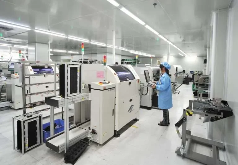
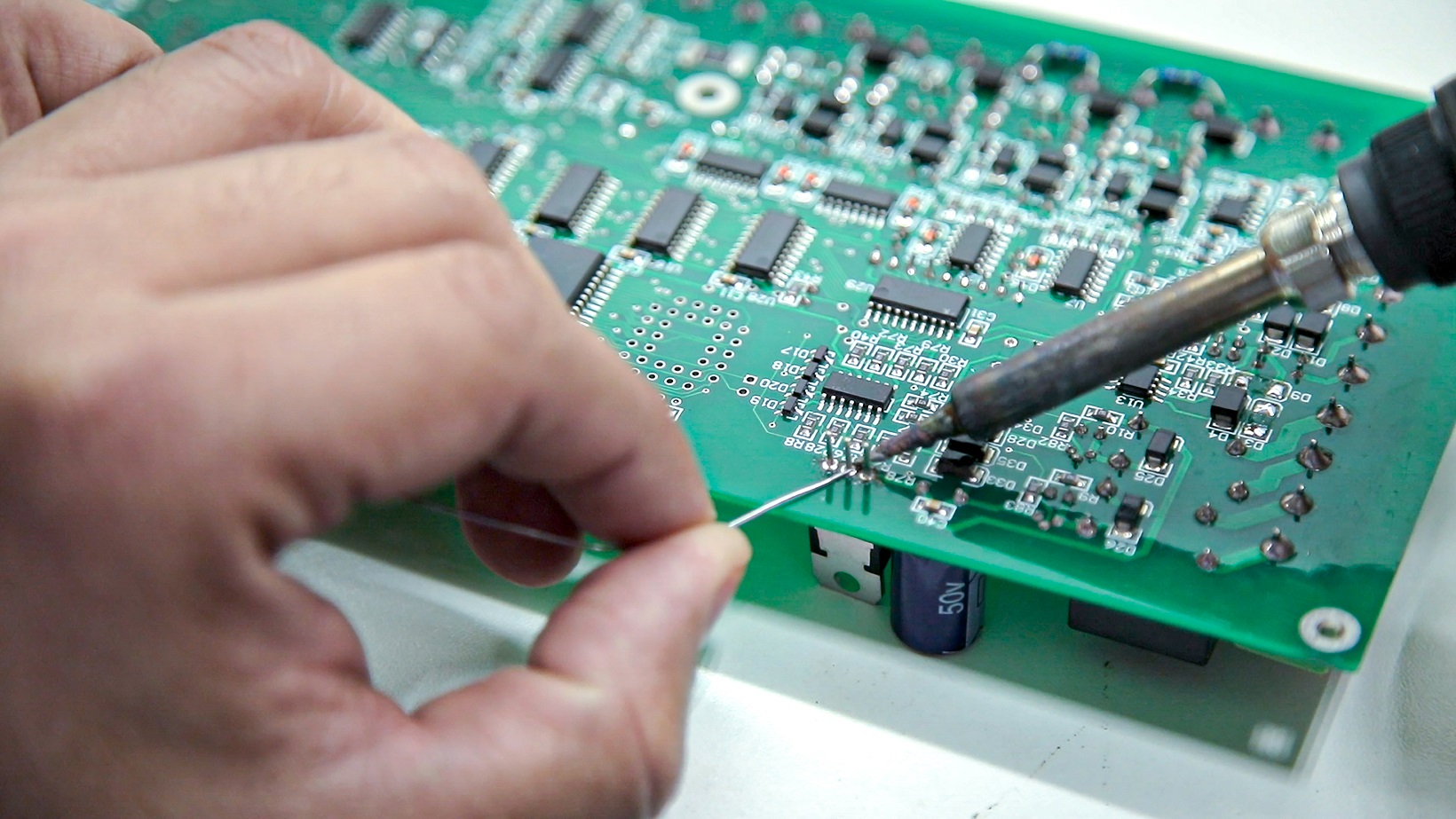
Printed Circuit Boards (PCBs) form the foundation of virtually all modern electronic devices, from consumer gadgets to mission-critical systems in aerospace and medical fields. The soldering process is what transforms a bare board and loose components into a functional assembly by creating strong, conductive joints between component leads/pads and copper traces. Mastering different soldering techniques and recognizing common defects early can dramatically improve yield rates, reduce rework costs, and enhance product reliability.
This blog explores the major soldering methods used in SMT PCB assembly today, the underlying principles, their strengths and limitations, and the most frequent defects that can occur. We'll cover through-hole and surface-mount approaches, automated versus manual processes, and practical strategies for defect prevention and correction.
Fundamentals of Soldering in PCB Assembly
Soldering relies on creating a metallurgical bond using a low-melting-point alloy (typically tin-based, with or without lead) that flows when heated and solidifies to form an electrical and mechanical connection. Flux plays a critical role by removing oxides, promoting wetting, and protecting the joint during cooling.
Key variables include:
- Temperature control — Precise profiles prevent overheating or underheating.
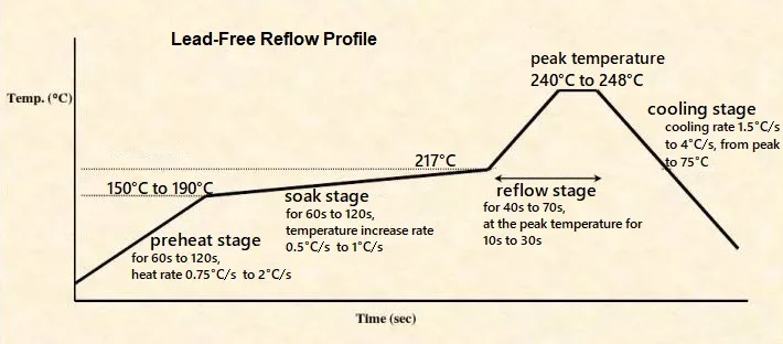
- Solder alloy selection — Lead-free options like SAC305 require higher temperatures (~217–220°C melting point).
- Surface preparation — Clean pads and leads ensure good wetting.
- Process type — Through-hole for mechanical strength vs. SMT for density.
Common inspection standards like IPC-A-610 define acceptable joint appearance: shiny, concave fillets with full wetting. Defects often arise from imbalances in these factors, leading to issues like poor adhesion, high resistance, or mechanical failure.
Mastering Wave Soldering: Process Control and Defect Resolution
Wave soldering remains highly efficient for high-volume through-hole assemblies. Boards move on a conveyor through fluxing, preheating (100–150°C), and contact with a turbulent solder wave (250–260°C), forming joints simultaneously.
While fast and consistent, it demands tight control of parameters like wave height, conveyor speed, flux activity, and solder purity to avoid issues.
Frequent challenges include incomplete hole filling, excess solder formations, and poor wetting, often tied to preheat inconsistencies or contamination.
Discover practical parameter settings, maintenance schedules, and step-by-step solutions for typical problems in: Troubleshooting Wave Soldering Defects: A Guide for PCB Assembly Engineers.
Avoiding Component Lift-Off Issues in SMT Assembly
One of the most frustrating SMT defects involves chip components standing upright on one pad during reflow, creating open circuits. This phenomenon stems from unbalanced wetting forces caused by asymmetric heating, uneven solder paste volume, or mismatched pad geometries.
Reflow ovens follow strict profiles: preheat, soak, peak reflow, and controlled cooling. Small imbalances become amplified in high-density designs.
Prevention focuses on symmetrical pad layouts (per IPC-7351), uniform stencil printing, balanced thermal mass around pads, and optimized reflow ramps (1–3°C/s).
Learn comprehensive strategies including design rules, process tweaks, and material choices to eliminate this defect: Preventing Tombstoning: A Guide to Flawless PCB Assembly.
Identifying and Repairing Cold Solder Joints with Hot Air Techniques
Cold joints appear dull, grainy, or cracked due to inadequate heat, movement during solidification, or surface contamination, resulting in unreliable connections prone to failure under vibration or thermal cycling.
Visual cues include poor fillet formation and matte appearance, while electrical tests reveal high resistance.
Hot air rework stations offer effective repair by delivering uniform heat to reflow the joint without excessive localized stress. Proper technique involves flux addition, controlled temperature/airflow (300–350°C), and gentle nozzle movement.
For expert diagnosis tips, step-by-step rework procedures, and long-term prevention advice, refer to: Troubleshooting Cold Solder Joints: Hot Air Rework to the Rescue!.
Additional Prevalent Soldering Defects and Prevention Tactics
Beyond the core topics above, other common issues include:
- Bridging and shorts — Excess solder connecting adjacent pins; mitigated by optimized wave height or mask design.
- Solder balls/beads — Spatter from flux volatiles; controlled via paste formulation and reflow atmosphere.
- Voids — Gas pockets in joints; reduced through vacuum reflow or better flux outgassing.
- Insufficient wetting — Poor flow; addressed by surface cleanliness and flux activity.
Industry standards (IPC, SMTA) emphasize root cause analysis using tools like X-ray, cross-sectioning, and AOI.
Soldering Defect Troubleshooting: Diagnose, Fix, and Prevent Common Solder Joint Issues
Even with optimized processes and strong preventive measures, solder joint defects can still arise from minor variations in materials, equipment calibration, environmental factors, or operator differences. When issues surface during production or inspection, fast and accurate diagnosis plus targeted rework becomes essential to salvage boards, sustain throughput, and stop problems from repeating.
Key defects commonly seen across SMT, wave, and selective soldering include:
- Solder bridging — Unintended shorts between adjacent pads or pins, typically caused by excess paste, stencil misalignment, or placement inaccuracies.
- Solder balling — Scattered small solder spheres on the board surface, often due to moisture in paste, flux splatter, or overly aggressive reflow profiles.
- Insufficient wetting — Incomplete solder spread and fillet formation, resulting in weak or open joints from surface oxidation, poor flux activity, or inadequate heat transfer.
- Related problems like cold joints (dull, grainy appearance), tombstoning (detailed earlier), and cracked joints from thermal or mechanical stress.
A systematic troubleshooting process begins with layered inspection methods:
- Visual and magnified inspection — Identify surface issues such as bridging strands, stray balls, or poor wetting, following IPC-A-610 criteria.
- Automated Optical Inspection (AOI) — Enables high-speed detection of visible defects in high-volume lines.
- X-ray imaging — Critical for uncovering hidden defects (e.g., voids, head-in-pillow in BGAs, or non-wetted interfaces under components).
- Electrical and functional testing — Verifies opens, shorts, or high-resistance paths that affect performance.
After diagnosis, implement precise corrective actions:
- For bridging: Remove excess solder with desoldering braid, wick, or vacuum tools, clean thoroughly, then re-apply solder under controlled conditions.
- For balling: Clean affected areas with isopropyl alcohol and soft brushing; optimize reflow atmosphere and paste storage/handling to minimize volatiles.
- For insufficient wetting: Apply additional flux, reheat using a soldering iron or hot air (respecting component thermal limits), and confirm proper surface preparation and cleanliness.
For deeper root cause analysis, visual examples of defects, detailed step-by-step rework instructions, inspection tool best practices, and engineer-focused insights aligned with IPC standards (e.g., IPC-A-610H, J-STD-001H), check out our in-depth guide: Soldering Troubleshooting: Diagnosing and Fixing Common Solder Joint Issues
Mastering these diagnostic and repair skills helps assembly teams resolve issues quickly, cut down on scrap and rework expenses, and foster ongoing improvements in PCB manufacturing reliability.
Best Practices for Reliable Soldering Outcomes
Achieving near-zero defects requires:
- DFM reviews early in design.
- Calibrated equipment and regular maintenance.
- Process monitoring with SPC.
- Multi-level inspection (visual, AOI, X-ray, functional testing).
- Operator training and ESD protection.
Integrating these practices across processes significantly boosts first-pass yield.
Future Trends in PCB Soldering Technology
The soldering landscape continues to evolve with emerging trends including:
- Low-temperature solders reducing thermal stress on components
- Advanced flux formulations improving wetting and reducing residue
- Laser soldering for ultra-precise localized heating
- AI-assisted inspection systems for real-time defect detection
- Environmentally sustainable materials meeting evolving regulations
Conclusion: Building Reliability Through Soldering Excellence
The reliability, performance, and longevity of any printed circuit board ultimately depend on the quality of its solder joints. Well-executed soldering ensures robust electrical connectivity, mechanical stability, and resistance to environmental stresses across the PCB's lifecycle—from prototyping to field deployment.
By understanding the strengths and limitations of various soldering processes, proactively addressing common defects, and applying targeted prevention and rework strategies, manufacturers can significantly reduce failure rates, minimize costly rework, and achieve higher first-pass yields. Whether you're working with selective soldering for mixed-technology boards, optimizing wave soldering parameters, or perfecting SMT reflow profiles, continuous improvement in soldering quality remains fundamental to electronic manufacturing success.


