Introduction
To appreciate the advantages of Plated Through-Holes, it is crucial to understand their distinction from Non-Plated Through-Holes (NPTH). Both are holes drilled through the PCB substrate, but their functionality differs fundamentally.
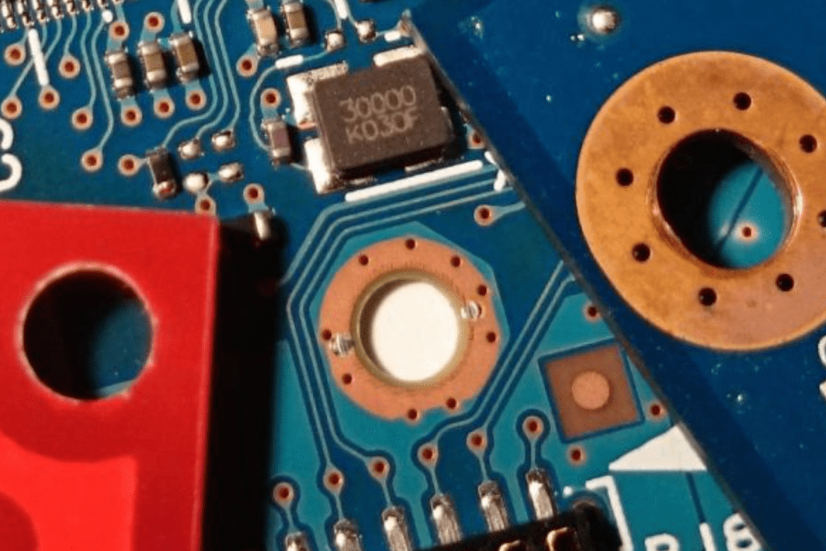
A Plated Through-Hole (PTH) is a hole drilled through the PCB that has its barrel electroplated with a conductive material, typically copper. This plating creates an electrical connection between the conductive layers that the hole passes through. PTHs serve two primary functions: providing electrical pathways between different layers of a multilayer PCB and offering robust mounting points for through-hole components. For instance, a component lead inserted into a PTH will solder to the plated barrel, creating a strong electrical and mechanical joint.
In contrast, a Non-Plated Through-Hole (NPTH) is simply a drilled hole without any conductive material deposited on its walls. NPTHs are typically used for mechanical purposes, such as mounting holes for securing the PCB to an enclosure, or for alignment pins. They do not establish any electrical connection between layers. The choice between PTH vs NPTH is therefore driven by the functional requirement: electrical connectivity for PTHs, and purely mechanical for NPTHs. For complex board assemblies, the extensive use of PTHs is what enables advanced circuit designs and component integration.
Related Reading: Optimizing Plated Through-Hole Design for High-Speed PCB Performance
The PTH Fabrication Process: Building Conductivity and Strength
The fabrication process for PTHs is a critical sequence that transforms a simple drilled hole into a reliable electrical conduit. This multi-step process requires precision and adherence to strict manufacturing standards to ensure the final PTH reliability.
Drilling
The process begins with mechanically drilling holes through the copper-clad laminate. The drill bits must be precise to achieve the specified hole diameter and position.
Desmear/Etchback
After drilling, a chemical process called desmear (or etchback) is applied. This removes resin smears that might have been deposited on the copper foil during drilling, ensuring that the subsequent plating adheres directly to clean copper layers. This step is vital for robust electrical connections.
Electroless Copper Deposition
A very thin layer of electroless copper is chemically deposited onto the entire surface of the PCB, including the walls of the drilled holes. This initial copper layer is non-electrolytic and provides a conductive base, preparing the hole walls for the subsequent electrolytic plating step.
Electrolytic Copper Plating
This is the most critical step for building up the PTH current carrying capacity and mechanical strength. The PCB is submerged in an electrolytic copper bath, and an electric current is passed through it. Copper ions are attracted to and deposited onto the electroless copper layer, building up a thicker, robust copper barrel inside the hole. This plating thickness is carefully controlled to meet design specifications, typically 20 to 25 micrometers (µm) as per IPC-6012E, "Qualification and Performance Specification for Rigid Printed Boards," depending on the product's performance class.
Surface Finish Application
Finally, a surface finish (e.g., tin, gold, OSP) is applied over the exposed copper on the pads and within the PTH to protect the copper from oxidation and ensure solderability during component assembly.
This meticulous PTH fabrication process ensures that each PTH is electrically continuous, robust, and ready for reliable component assembly.
Enhanced PTH Reliability Through Plating
One of the foremost benefits of PTHs is the significantly enhanced PTH reliability they offer to PCB assemblies. This reliability stems from both electrical and mechanical advantages that non-plated holes cannot provide.
Electrically, the plated copper barrel in a PTH creates a robust, low-resistance connection between all connected layers of the PCB. This eliminates the need for solder fillets to carry current through the board thickness, which can be inconsistent or prone to failure. The consistent and controlled plating thickness ensures a predictable electrical path, crucial for signal integrity and minimizing voltage drops. This contributes directly to the overall functional stability of the PCB.
Mechanically, the copper plating strengthens the walls of the through-hole. When through-hole components are inserted and soldered into PTHs, the solder flows into the plated barrel, creating a strong metallurgical bond with the copper. This connection provides superior mechanical support for the component, making the assembly more resistant to vibration, shock, and thermal cycling. For example, large or heavy components benefit greatly from this added mechanical integrity, preventing lead fatigue or detachment. The acceptability criteria for these soldered connections are detailed in standards like IPC-A-610G, "Acceptability of Electronic Assemblies," which emphasizes the importance of good barrel fill and wetting for long-term reliability.
PTH Current Carrying Capacity and Thermal Management
The copper plating within a PTH directly contributes to its superior PTH current carrying capacity and improved thermal management capabilities, which are crucial for power applications and heat dissipation.
The plated copper barrel acts as an efficient conductor, allowing a significantly higher current to pass through the hole compared to an unplated hole where current would primarily rely on solder or friction. The amount of current a PTH can safely carry is directly proportional to its diameter and the plating thickness. Thicker copper plating provides a larger cross-sectional area for current flow, reducing resistance and thus minimizing heat generation within the hole. This is especially important for power delivery networks where high currents need to be distributed across different layers of the PCB. Design guidelines often specify minimum copper plating thickness based on the expected current, as referenced in IPC-2221B, "Generic Standard on Printed Board Design."
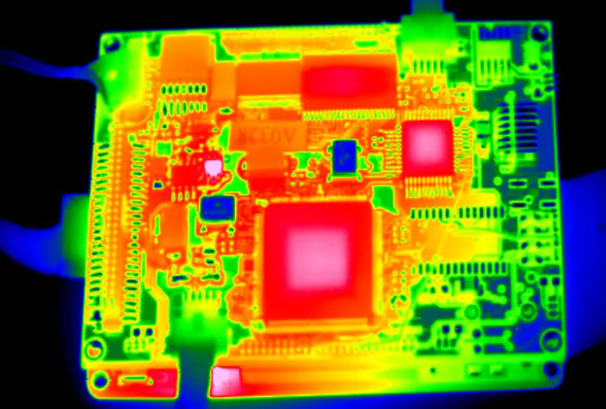
Beyond just current flow, the copper plating in PTHs also assists in thermal management. Copper is an excellent thermal conductor. Heat generated by components on one side of the board can be effectively dissipated to other layers or to external heat sinks via the thermally conductive PTH barrels. In many designs, an array of PTHs, sometimes referred to as "thermal vias," is strategically placed under or near heat-generating components to actively transfer heat away, preventing localized hot spots that could degrade component performance or reliability. This dual benefit of enhanced electrical conductivity and thermal dissipation makes PTHs indispensable in modern electronic designs.
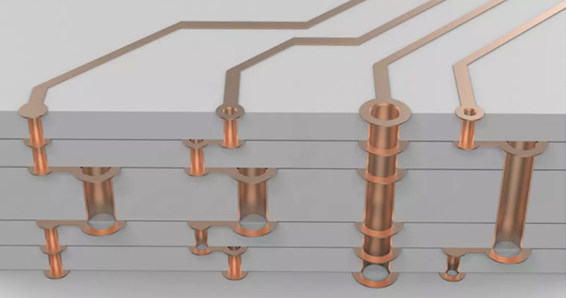
PTH in Multilayer PCBs: Enabling Complexity
The role of PTHs in multilayer PCBs is perhaps their most defining benefit, enabling the creation of compact, complex, and high-performance electronic circuits that would be impossible with simpler board constructions.
In a multilayer PCB, conductive traces and planes are sandwiched between layers of insulating material. PTHs serve as the essential vertical interconnections, allowing signals and power to traverse from one layer to any other layer within the board. Without PTHs, connecting internal layers would necessitate much larger, less efficient routing strategies or even separate boards. This capability is fundamental for achieving high component density and intricate circuit designs, which are hallmarks of modern electronics.
For example, in a 10-layer board, a single PTH can connect a signal from the top layer to an internal signal layer, then to an internal power plane, and finally to the bottom layer. This efficient use of vertical space is what allows designers to pack more functionality into smaller form factors, reduce signal path lengths, and improve overall system performance. The precise control over the PTH fabrication process ensures these interconnections are reliable, even in boards with many layers and high aspect ratios (ratio of board thickness to hole diameter). The structural integrity provided by PTHs also supports the complex stacking of layers, maintaining the overall mechanical stability of the board.
Related Reading: Solving Plated Through-Hole Problems: A PCB Troubleshooting Guide
Conclusion
Plated Through-Holes are far more than just holes in a PCB; they are foundational elements that underpin the electrical and mechanical integrity of electronic assemblies. By offering significant advantages over NPTHs, the meticulous PTH fabrication process ensures a robust and reliable connection. These plated structures enhance PTH reliability by providing strong electrical and mechanical bonds for components, boost PTH current carrying capacity, and aid in thermal management. Critically, PTHs in multilayer PCBs are the essential enablers of complex circuit designs, allowing for high-density routing and efficient vertical interconnections. Understanding and properly specifying PTHs are therefore paramount for any engineer or designer aiming to produce high-quality, high-performance PCB assemblies.
FAQs
Q1: What is the primary difference between a PTH and an NPTH?
A1: The primary difference is that a Plated Through-Hole (PTH) has a conductive material, typically copper, plated on its barrel, providing an electrical connection between layers. A Non-Plated Through-Hole (NPTH) has no plating and serves purely mechanical purposes, lacking electrical conductivity, which is key for PTH vs NPTH understanding.
Q2: How does the PTH fabrication process contribute to board reliability?
A2: The PTH fabrication process, involving drilling, desmear, and precisely controlled electroless and electrolytic copper plating, builds a robust, conductive barrel. This process ensures strong electrical connections between layers and enhances the mechanical integrity for component mounting, directly contributing to overall PTH reliability in PCB assembly.
Q3: Why are PTHs crucial for high PTH current carrying capacity?
A3: PTHs are crucial for high PTH current carrying capacity because the copper plating inside the hole provides a low-resistance pathway for current to flow between layers. The thickness of this copper plating directly influences the amount of current the PTH can safely carry without excessive heat generation, making them essential for power distribution in PCB assembly.
Q4: What is the significance of PTH in multilayer PCBs?
A4: PTH in multilayer PCBs is highly significant as it provides the essential vertical interconnections between internal and external layers. This allows for complex circuit routing in compact spaces, enabling high-density component placement and intricate designs, which are fundamental to the functionality and performance of modern multilayer PCB assemblies.
References
IPC-A-610G — Acceptability of Electronic Assemblies. IPC, 2017.
IPC-6012E — Qualification and Performance Specification for Rigid Printed Boards. IPC, 2017.
IPC-2221B — Generic Standard on Printed Board Design. IPC, 2012.
ISO 9001:2015 — Quality Management Systems. ISO, 2015.


