Introduction
Through-hole components have long been a staple in printed circuit board (PCB) assembly, valued for their mechanical strength and reliability in high-stress applications. While surface mount technology (SMT) dominates modern electronics, through-hole components remain essential for power electronics, connectors, and legacy designs. Reflow soldering, typically associated with SMT, is increasingly adapted for through-hole assembly to streamline mixed-technology boards. This article explores through-hole reflow techniques, focusing on innovative approaches like variable thickness stencils and optimized solder paste techniques. Aimed at electrical engineers, this discussion provides practical insights into achieving robust solder joints while adhering to industry standards. The goal is to enhance process efficiency and ensure reliability in diverse PCB applications by addressing the unique challenges of through-hole reflow soldering.
What Is Through-Hole Reflow and Why It Matters
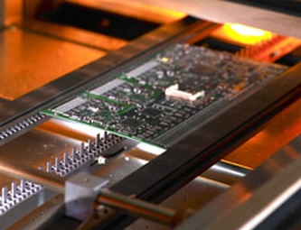
Through-hole reflow soldering refers to a process where through-hole components are soldered to a PCB using a reflow oven, traditionally used for SMT components. In this method, solder paste is applied to the through-hole pads and inside the plated-through holes, and components are inserted before the board undergoes controlled heating. The solder paste melts and forms a permanent joint as it cools, securing the component leads.
This technique matters because it allows manufacturers to combine SMT and through-hole components on a single board without requiring separate wave soldering processes. It reduces production steps, lowers costs, and improves throughput in assembly lines. For electrical engineers working on mixed-technology designs, through-hole reflow offers a solution to maintain design flexibility while meeting stringent reliability requirements. It is particularly relevant for applications where thermal and mechanical stresses demand the durability of through-hole joints.
Technical Principles of Through-Hole Reflow Soldering
Through-hole reflow soldering relies on precise control of solder paste application and thermal profiles to ensure proper wetting and joint formation. Unlike wave soldering, where molten solder flows over the board, reflow soldering depends on the pre-applied solder paste to create the connection. The process involves several key principles.
First, solder paste must be deposited not only on the pad surface but also within the plated-through hole to ensure sufficient material for a strong joint. This requires careful SMT stencil design to control paste volume. Second, the thermal profile in the reflow oven must account for the mass of through-hole components, which often have larger leads and require more heat to achieve proper solder flow. The profile typically includes preheat, soak, reflow, and cooling zones, each tailored to prevent thermal shock and ensure even heating.
Another critical factor is capillary action, which draws molten solder into the through-hole during reflow. This action depends on the hole size, lead diameter, and solder paste composition. Standards such as IPC J-STD-001H provide guidelines for acceptable joint formation, emphasizing complete fillet formation around the lead on both sides of the board.
Challenges arise due to the differences in thermal mass between through-hole and SMT components. Uneven heating can lead to insufficient solder flow or component damage. Engineers must balance the reflow profile to meet the needs of all components on the board while adhering to thermal limits specified in standards like JEDEC J-STD-020E for moisture-sensitive devices.
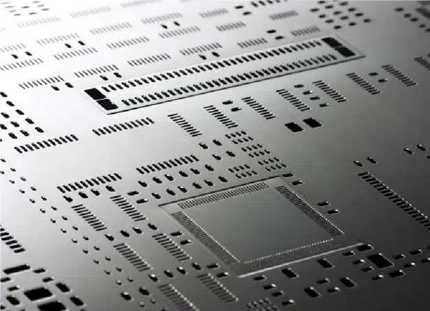
Variable Thickness Stencils in Through-Hole Reflow
Variable thickness stencils, also known as stepped stencils, are a specialized tool in through-hole reflow soldering. These stencils feature areas of different thicknesses to control the amount of solder paste deposited on specific regions of the PCB. For through-hole components, a thicker stencil area over the through-hole pads and holes allows for a higher volume of solder paste, ensuring adequate material for joint formation.
The principle behind variable thickness stencils is to address the unique solder volume requirements of through-hole components compared to SMT pads. Standard stencils with uniform thickness often result in insufficient paste for through-hole joints, leading to weak connections or voids. By increasing stencil thickness in targeted areas, typically by 0.05 to 0.1 millimeters more than the surrounding SMT areas, engineers can deposit the necessary paste volume without over-applying to smaller pads.
Implementing variable thickness stencils requires precise design and fabrication. The stencil apertures for through-hole pads are often oversized compared to the pad dimensions to allow paste to flow into the hole. Guidelines from IPC-7525B, which covers stencil design, recommend adjusting aperture size and shape based on component type and hole diameter to optimize paste transfer. This approach minimizes defects like insufficient fill or solder bridging during reflow.
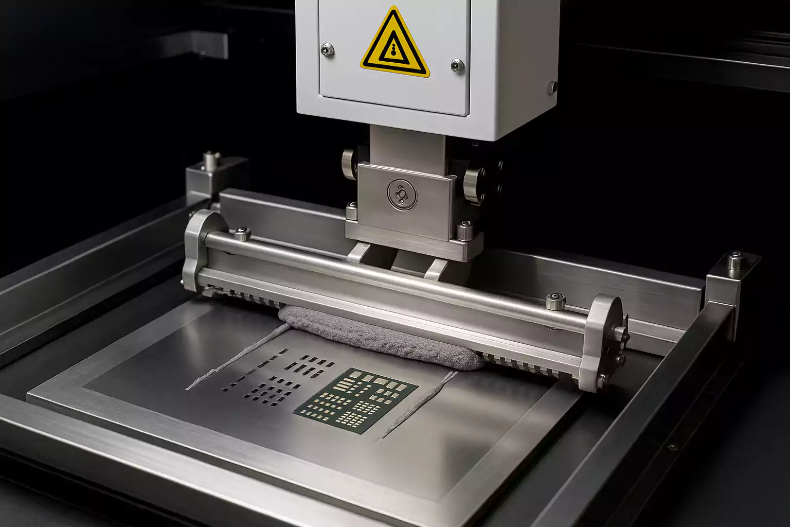
Solder Paste Techniques for Through-Hole Reflow
Solder paste techniques play a vital role in achieving reliable through-hole reflow joints. The paste, a mixture of solder alloy particles and flux, must be selected and applied with precision to ensure proper melting and wetting. Several factors influence the effectiveness of solder paste in this context.
The composition of the solder paste is critical. Lead-free alloys, often based on tin-silver-copper, are common due to environmental regulations. The particle size of the solder powder, typically classified as Type 3 or Type 4 per IPC J-STD-005A, affects printability and flow into through-hole barrels. Smaller particles improve paste transfer for fine-pitch SMT components, while larger particles may be better for through-hole applications requiring more volume.
Application methods also matter. Overprinting is a common technique where the stencil aperture is designed to deposit extra paste around and into the through-hole. This ensures enough material is available for capillary action during reflow. Additionally, the flux activity level must be sufficient to clean oxides from the lead and hole surfaces, promoting wetting. Standards like IPC J-STD-004B classify flux types and activity levels, guiding engineers in selecting the appropriate paste for their process.
Thermal profiling complements solder paste techniques. A well-designed profile ensures the paste reaches its liquidus temperature, allowing full flow into the hole without overheating nearby components. Engineers often use a longer soak zone in the profile to preheat through-hole components evenly before the reflow peak.
Best Practices for Through-Hole Reflow Soldering
Achieving consistent results with through-hole reflow soldering requires adherence to best practices grounded in industry standards. These practices focus on design, process control, and inspection to minimize defects and ensure reliability.
Start with PCB and component design. Hole sizes must match component lead diameters per tolerances outlined in IPC-2221C, which provides generic standards for PCB design. Proper clearance ensures solder can flow into the hole without obstruction. Pad dimensions should also allow for sufficient paste deposition without risking bridging.
Stencil design is equally important. Use variable thickness stencils where possible to balance paste volume between SMT and through-hole areas. Follow guidelines from IPC-7525B for aperture sizing, ensuring overprinting for through-hole pads. Regularly inspect stencils for wear or clogging to maintain consistent paste transfer.
Process control during reflow is critical. Develop a thermal profile that accounts for the thermal mass of through-hole components. Monitor peak temperatures and time above liquidus to comply with JEDEC J-STD-020E for component safety. Use thermocouples on test boards to verify profile accuracy across different zones of the PCB.
Post-reflow inspection ensures joint quality. Visual inspection per IPC-A-610H criteria checks for fillet formation, wetting, and voiding. X-ray inspection may be necessary for hidden joints to detect insufficient fill or voids within the through-hole barrel. Address any defects by adjusting paste volume, stencil design, or reflow parameters.
Troubleshooting Common Issues in Through-Hole Reflow
Even with careful planning, issues can arise during through-hole reflow soldering. Identifying and resolving these problems is essential for maintaining PCBA assembly quality. Below are common challenges and solutions based on practical experience.
Insufficient solder fill in through-holes often results from inadequate paste volume or poor capillary action. Increase paste deposition by adjusting stencil apertures or using a thicker stencil section for through-hole areas. Verify hole and lead cleanliness, as contamination can hinder wetting. Refer to IPC J-STD-001H for acceptable fill criteria, typically requiring at least 75 percent vertical fill.
Solder voids within the through-hole barrel can compromise joint strength. Voids often stem from outgassing during reflow or trapped flux residues. Use a solder paste with appropriate flux activity per IPC J-STD-004B, and extend the preheat zone in the thermal profile to allow gases to escape before solder solidification.
Component misalignment or tombstoning may occur if thermal gradients are uneven across the board. Ensure the reflow profile provides gradual heating, especially for mixed-technology boards. Secure components with adhesive if necessary before reflow to prevent movement.
Conclusion
Through-hole reflow soldering offers a powerful solution for assembling mixed-technology PCBs, combining the reliability of through-hole components with the efficiency of reflow processes. By leveraging techniques like variable thickness stencils and optimized solder paste application, electrical engineers can achieve robust joints while streamlining production. Adherence to industry standards ensures process consistency and product reliability across applications. With careful attention to design, process control, and inspection, through-hole reflow can meet the demands of modern electronics manufacturing, providing a versatile approach for diverse PCB designs.
FAQs
Q1: What are the benefits of using through-hole reflow over traditional wave soldering?
A1: Through-hole reflow simplifies assembly by allowing mixed SMT and through-hole components to be soldered in a single process. It reduces production steps, cuts costs, and eliminates the need for separate wave soldering equipment. This method also minimizes thermal stress on boards by avoiding multiple heating cycles, improving overall reliability for electrical engineers working on complex designs.
Q2: How do variable thickness stencils improve through-hole reflow outcomes?
A2: Variable thickness stencils enhance through-hole reflow by depositing more solder paste in through-hole areas compared to SMT pads. Thicker stencil sections over holes ensure sufficient paste volume for strong joints. This tailored approach prevents insufficient fill or weak connections, offering engineers precise control over solder distribution during the assembly process.
Q3: What solder paste techniques are most effective for through-hole reflow soldering?
A3: Effective solder paste techniques for through-hole reflow include overprinting to deposit extra paste into holes and selecting paste with suitable particle size and flux activity. Overprinting ensures enough material for capillary action, while proper flux cleans surfaces for better wetting. Engineers should match paste properties to process needs for optimal joint formation.
Q4: How can engineers prevent voids in through-hole reflow joints?
A4: Preventing voids in through-hole reflow joints involves using solder paste with adequate flux to reduce outgassing and extending preheat time in the reflow profile. This allows trapped gases to escape before solder solidifies. Inspecting hole cleanliness and optimizing paste volume also minimizes void formation, ensuring reliable connections in PCB assemblies.
References
IPC J-STD-001H — Requirements for Soldered Electrical and Electronic Assemblies. IPC, 2021.
IPC-7525B — Stencil Design Guidelines. IPC, 2012.
IPC J-STD-005A — Requirements for Soldering Pastes. IPC, 2012.
IPC J-STD-004B — Requirements for Soldering Fluxes. IPC, 2011.
JEDEC J-STD-020E — Moisture/Reflow Sensitivity Classification for Nonhermetic Surface Mount Devices. JEDEC, 2014.
IPC-2221C — Generic Standard on Printed Board Design. IPC, 2021.
IPC-A-610H — Acceptability of Electronic Assemblies. IPC, 2021.


