Introduction
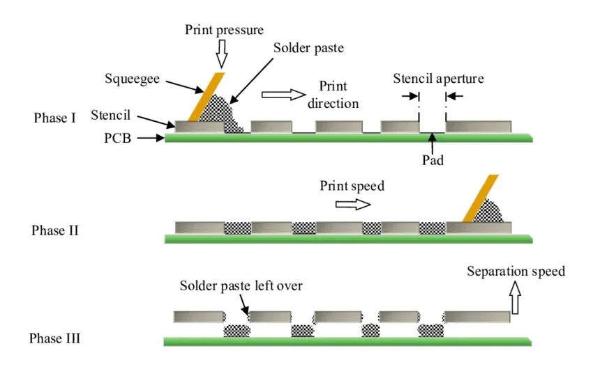
In surface mount technology assembly, stencils serve as the precise tool for depositing solder paste onto PCB pads, directly influencing assembly yield and reliability. Selecting the right stencil material among options like stainless steel, nickel, and Mylar can make or break your project's success by affecting paste release, aperture definition, and overall stencil durability. Engineers often face challenges such as inconsistent prints or premature wear, which stem from mismatched material choices. This masterclass dives into stencil materials, their properties, and practical selection criteria tailored for electric engineers tackling real-world PCB projects. By understanding these factors, you can optimize print performance and minimize defects in production runs.
Why Stencil Materials Matter in PCB Assembly
Stencil materials determine how well solder paste transfers to pads, impacting first-pass yield and rework costs in high-volume manufacturing. Poor material selection leads to issues like insufficient paste volume for fine-pitch components or bridging in denser layouts. Stainless steel stencils excel in demanding environments due to their robustness, while nickel stencils offer superior edge quality for ultra-fine features. Mylar stencils, on the other hand, provide a budget-friendly entry for prototyping but fall short in repeated use. Industry standards like IPC-7525 outline guidelines for stencil fabrication, emphasizing material properties for consistent performance. Ultimately, the right stencil material aligns with your PCB's pitch, volume, and paste type to ensure reliable assembly outcomes.
The relevance extends to troubleshooting common defects, where stencil durability plays a pivotal role in maintaining aperture integrity over thousands of prints. Engineers must evaluate how materials handle cleaning cycles, pressure variations, and chemical exposure from solder pastes. A mismatched stencil can amplify problems like paste smearing or starvation, cascading into reflow soldering failures. By prioritizing stencil materials based on project specifics, teams reduce downtime and enhance process control. This foundational choice sets the stage for scalable production without compromising quality.
Technical Properties of Common Stencil Materials
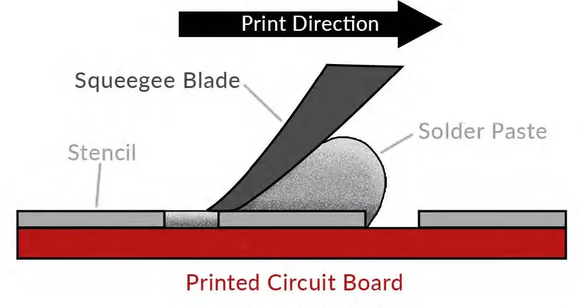
Stencil materials vary in composition, fabrication methods, and performance characteristics, each suited to specific PCB assembly needs. Stainless steel stencils, typically laser-cut or chemically etched, feature a robust structure that withstands high print pressures and frequent cleanings. Their surface can be polished or coated for improved paste release, making them a staple for mid-to-high volume runs. Nickel stencils, produced via electroforming, yield exceptionally smooth, vertical aperture walls ideal for pitches below 0.4 mm. Mylar stencils, made from polyester films, offer flexibility and low cost but limited thickness control. Understanding these properties helps engineers predict behavior under operational stresses.
Fabrication techniques further differentiate materials, influencing dimensional stability and edge quality. Laser cutting on stainless steel achieves tight tolerances but may leave tapered walls unless post-processed. Electroformed nickel naturally forms straight-sided apertures, enhancing volume transfer efficiency for micro-BGAs or QFNs. Polymer materials like Mylar rely on chemical etching or laser ablation, resulting in thinner profiles suitable for prototypes. Stencil durability emerges as a key metric, with stainless steel enduring over 100,000 prints in optimized setups, while nickel resists abrasion better in fine-feature applications.
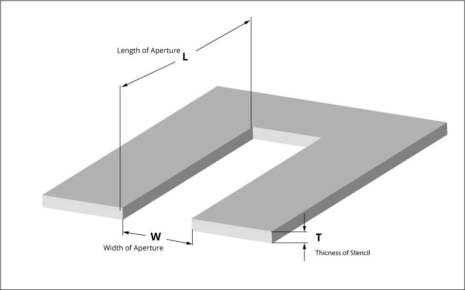
Surface finish and chemical resistance also factor into material performance during SMT processes. Stainless steel's grain structure can trap paste residues if not electropolished, potentially causing defects over time. Nickel provides a mirror-like finish that minimizes adhesion, promoting clean wipes and consistent deposits. Mylar's smooth but soft surface excels in low-abrasion scenarios yet degrades under aggressive solvents. These traits align with IPC-7525 recommendations for matching material to aperture aspect ratios and area ratios above 0.6 for optimal release.
Comparing Stencil Materials: Durability, Cost, and Application Fit
The following comparison highlights trade-offs in durability, cost, and application fit to guide material selection based on project demands:
- Stainless Steel Stencil - Durability: High (high-volume production); Cost: Moderate; Best For: Standard pitches, 0.5 mm+; Limitations: Tapered walls without polishing.
- Nickel Stencil - Durability: High (fine features); Cost: Higher; Best For: Ultra-fine pitch <0.4 mm; Limitations: Softer for extreme pressures.
- Mylar Stencil - Durability: Low (prototypes); Cost: Low; Best For: Low-volume, simple layouts; Limitations: Poor repeatability, thin limits.
Stainless steel stencils balance cost and durability for most assemblies, handling the rigors of automated lines. Nickel stencils shine where precision trumps volume, offering longevity in high-mix environments. Mylar suits quick-turn prototypes, avoiding capital outlay for infrequent use. Factors like frame type, whether framed or frameless, amplify these differences in handling and alignment.
In practice, stencil durability ties directly to lifecycle costs, as worn apertures lead to inconsistent paste heights and soldering defects per J-STD-001 criteria for soldered assemblies. Stainless steel resists deformation under squeegee pressure, extending usability in dirty paste environments. Nickel maintains edge sharpness longer for delicate components, reducing scrap rates. Mylar, prone to stretching, demands frequent replacement but accelerates early validation. Engineers should audit these attributes against production forecasts for cost-effective choices.
Best Practices for Selecting the Right Stencil Material
Start by assessing component pitch and aperture size to match material strengths, consulting IPC-7525 for design guidelines on thickness and reductions. For pitches above 0.5 mm and volumes over 1,000 units, opt for a stainless steel stencil with electropolishing to boost durability and release. Fine-pitch designs under 0.3 mm benefit from nickel electroforming, ensuring vertical walls for uniform paste volume. Prototype runs or budget constraints favor Mylar stencils, paired with manual printing for validation. Always factor in solder paste rheology, as type 4 or finer pastes pair best with smoother nickel surfaces.
Implement a selection checklist: evaluate production volume, cleaning frequency, and printer capabilities before committing. Test durability through accelerated wear trials, monitoring aperture wear after simulated cycles. Store stencils flat in controlled humidity to prevent warping, and clean with approved solvents to preserve material integrity. Hybrid approaches, like stainless steel with nickel overlays for critical areas, offer flexibility in mixed-technology boards. Regular inspection under magnification catches early degradation, averting yield drops.
Optimize printing parameters per material: lower pressures for Mylar to avoid tears, higher snap-off for stainless steel to ensure clean separation. Post-print verification with SPI equipment confirms material suitability before full runs. Document choices in process control plans, linking back to assembly performance metrics.
Troubleshooting Stencil Material Issues in Production
Common defects like solder bridging often trace to inadequate paste release from rough stainless steel surfaces, resolved by polishing or switching to nickel for smoother walls. Insufficient paste volume in fine apertures signals mismatched thickness, where nickel stencils excel due to precise electroforming. Mylar stencils frequently cause smearing from flexing, best mitigated by rigid framing or relegating to low-speed prototypes. Durability failures may manifest as rounded apertures after 50,000 prints on stainless steel, prompting recoating or replacement.
Paste starvation on QFN exposed pads points to trapped residues in stainless steel grains, demanding ultrasonic cleaning protocols. Nickel stencils mitigate this with inherent non-stick properties but may dent under excessive pressure, requiring printer adjustments. Mylar's low durability leads to tears in high-finesse areas, necessitating redesign for polymer limits. Cross-reference defects against J-STD-001 acceptance criteria to isolate material contributions.
Layered troubleshooting involves material swaps: test nickel for persistent fine-pitch issues after stainless steel underperforms. Monitor wipe frequency, as over-wiping accelerates wear across materials. Collaborate with assembly teams to log defect paretos, refining selections iteratively.
Conclusion
Mastering stencil materials empowers electric engineers to achieve precise, reliable PCB assembly by aligning choices with project specifics. Stainless steel stencils deliver robust durability for production, nickel stencils precision for fine features, and Mylar stencils economy for prototypes. Adhering to standards like IPC-7525 ensures consistent outcomes, minimizing defects and costs. Prioritize factors such as pitch, volume, and process controls in your decisions. With these insights, optimize your next project for superior yield and performance.
FAQs
Q1: What factors determine stencil durability in high-volume PCB assembly?
A1: Stainless steel stencils offer superior durability for high-volume runs due to resistance to wear from squeegee pressure and frequent cleaning. Nickel stencils provide strong longevity for fine-pitch applications, with smooth walls reducing abrasion. Consider production cycles, paste type, wipe frequency, and maintenance to extend life, avoiding over-wiping that accelerates degradation. Follow IPC-7525 for fabrication aligned with durability needs.
Q2: When should I choose a stainless steel stencil over a nickel stencil?
A2: Choose stainless steel for standard-pitch, high-volume projects when cost and robustness matter. It handles aggressive cleaning and higher pressures well, ensuring consistent prints. Nickel is preferred for ultra-fine features under 0.4 mm pitch, prioritizing edge quality and paste release over bulk durability. Evaluate layout density, paste type, and run size for the best fit.
Q3: Are Mylar stencils suitable for production PCB projects?
A3: Mylar stencils work best for prototypes or very low-volume builds due to low cost and ease of fabrication but lack durability for production. They flex under pressure, leading to inconsistent deposits and rapid wear. Use them for early validation, then switch to stainless steel or nickel for scalable assembly to maintain yield.
Q4: How do stencil materials affect solder paste printing quality?
A4: Stainless steel provides reliable volume transfer for most pastes, while nickel enhances release for fine apertures via smooth, vertical walls. Mylar carries higher risk of smearing due to flexibility but suits simple layouts. Match material to paste rheology and pitch per IPC guidelines to avoid bridging or starvation and to ensure defect-free reflow.
References
IPC-7525C - Stencil Design Guidelines. IPC, 2021
IPC J-STD-001J - Requirements for Soldered Electrical and Electronic Assemblies. IPC, 2024