Introduction
In the intricate world of printed circuit board assembly, achieving high solder joint quality during surface mount technology processes remains a priority for electrical engineers. A key tool in this endeavor is the step-down stencil, a specialized design used to control solder paste deposition on complex boards. This approach directly influences SMT assembly outcomes, particularly when it comes to PCB rework and repair tasks. By varying stencil thickness in specific areas, engineers can address challenges tied to component density and thermal profiles. This article explores how step-down stencils impact rework efficiency, repair precision, and overall reliability in SMT assembly. With a focus on practical implications, the discussion aims to equip professionals with insights into optimizing solder joint quality through informed stencil design choices.
What Is a Step-Down Stencil and Why It Matters
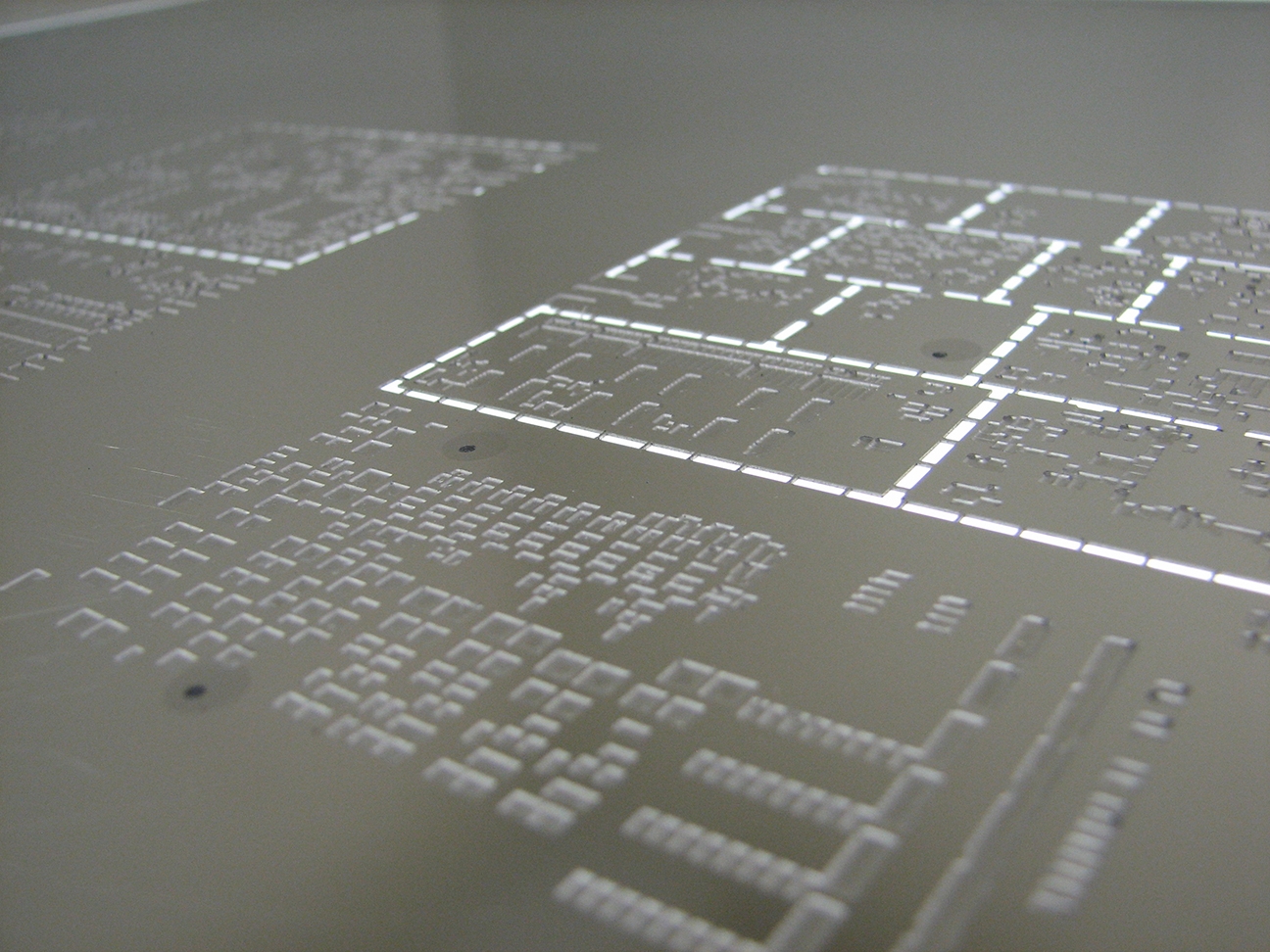
A step-down stencil is a type of SMT stencil with varying thicknesses across its surface, designed to deposit different volumes of solder paste on a single PCB. Typically, areas with finer pitch components require less paste, achieved by reducing stencil thickness in those zones. This customization ensures uniform soldering results across diverse component types. For electrical engineers, the significance lies in its ability to mitigate common assembly defects like bridging or insufficient solder, which are critical during high-density board production.
The relevance of step-down stencils becomes evident in rework and repair scenarios. When components fail or need replacement, consistent solder application during initial assembly reduces the likelihood of joint failures. This directly affects the ease of desoldering and resoldering tasks. Moreover, reliability in SMT PCB assembly hinges on precise paste deposition, making step-down stencils a vital tool for maintaining long-term board performance under operational stress.
Technical Principles of Step-Down Stencils in SMT Assembly
Step-down stencils operate on the principle of controlled solder paste volume. In standard stencils, uniform thickness often leads to excess paste on fine-pitch components, risking short circuits, or insufficient paste on larger components, causing weak joints. By contrast, step-down designs feature thinner sections, often reduced by 25 to 50 micrometers, for smaller components, while maintaining thicker areas for power devices or connectors. This variation aligns paste volume with component requirements, enhancing solder joint quality.
The mechanism also addresses thermal dynamics during reflow. Components with different thermal masses heat at varying rates. A tailored paste deposit ensures smaller components do not overheat or form cold joints, while larger ones receive adequate solder for robust connections. According to guidelines in IPC-7525B, SMT stencil Design Guidelines, such precision in paste application is essential for minimizing defects in mixed-technology boards. This standard emphasizes aperture design adjustments, which step-down stencils inherently support through thickness variations.
In rework contexts, initial assembly quality determines repair complexity. Poor solder joints from uneven paste application often crack or fail under thermal stress during desoldering. Step-down stencils reduce these risks by standardizing joint formation, ensuring rework involves less mechanical strain on the board.
Impact on PCB Rework and Repair Processes
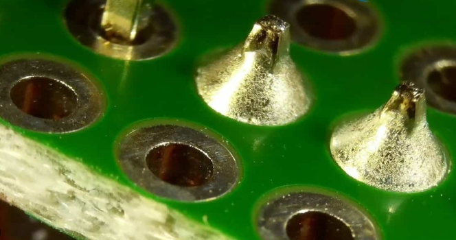
PCB rework involves removing and replacing defective components, while repair focuses on fixing damaged traces or joints. Both processes demand precision, as excessive heat or mechanical stress can degrade board integrity. Step-down stencils play a crucial role by ensuring initial solder joint quality, which simplifies these tasks. When joints are uniform and robust, desoldering requires less heat, reducing the risk of pad lifting or delamination.
Consider a scenario with fine-pitch components. Without a step-down stencil, excess paste can cause bridging, making component removal difficult. Engineers must spend additional time cleaning residues, risking damage to adjacent areas. With controlled paste deposition, joints remain clean and distinct, allowing for targeted rework. This efficiency is vital in high-reliability applications, such as aerospace or medical devices, where rework must not compromise overall board function.
Repair tasks also benefit from the initial assembly precision offered by step-down stencils. Damaged joints often stem from insufficient solder or voids, issues mitigated by proper paste volume. When repairs are needed, consistent joint formation ensures new solder bonds effectively with existing material, adhering to standards like IPC-7711/7721C, Rework, Modification and Repair of Electronic Assemblies. This standard highlights the importance of original assembly quality in successful repair outcomes.
Enhancing Solder Joint Quality and SMT Assembly Reliability
Solder joint quality is a cornerstone of SMT assembly reliability. Step-down stencils contribute by optimizing paste transfer efficiency. Fine-pitch areas receive just enough solder to form reliable connections without excess, while larger components get sufficient material for mechanical strength. This balance minimizes common defects like tombstoning or solder balls, which can lead to field failures.
Reliability extends beyond initial assembly to long-term performance. Boards assembled with step-down stencils exhibit fewer stress-related joint failures, as uniform solder distribution reduces thermal mismatch during operation. Standards such as IPC-A-610H, Acceptability of Electronic Assemblies, define criteria for joint appearance and integrity, which step-down stencil designs help achieve consistently. For engineers, this translates to fewer warranty claims or customer returns, a critical metric in competitive industries.
In high-density designs, where component spacing is minimal, reliability gains are even more pronounced. Step-down stencils prevent over-pasting, a frequent cause of short circuits in tight layouts. By aligning solder volume with design needs, these stencils support robust assembly processes, ensuring boards withstand environmental stresses like vibration or humidity over extended periods.
Practical Solutions for Implementing Step-Down Stencils
For electrical engineers looking to integrate step-down stencils into their workflow, several best practices ensure optimal results. First, collaborate with design teams to map component types and their solder requirements. Identify areas with fine-pitch devices versus larger components to define stencil thickness zones. Guidelines in IPC-7525B recommend aperture-to-pad ratios and thickness variations based on component pitch, providing a starting point for customization.
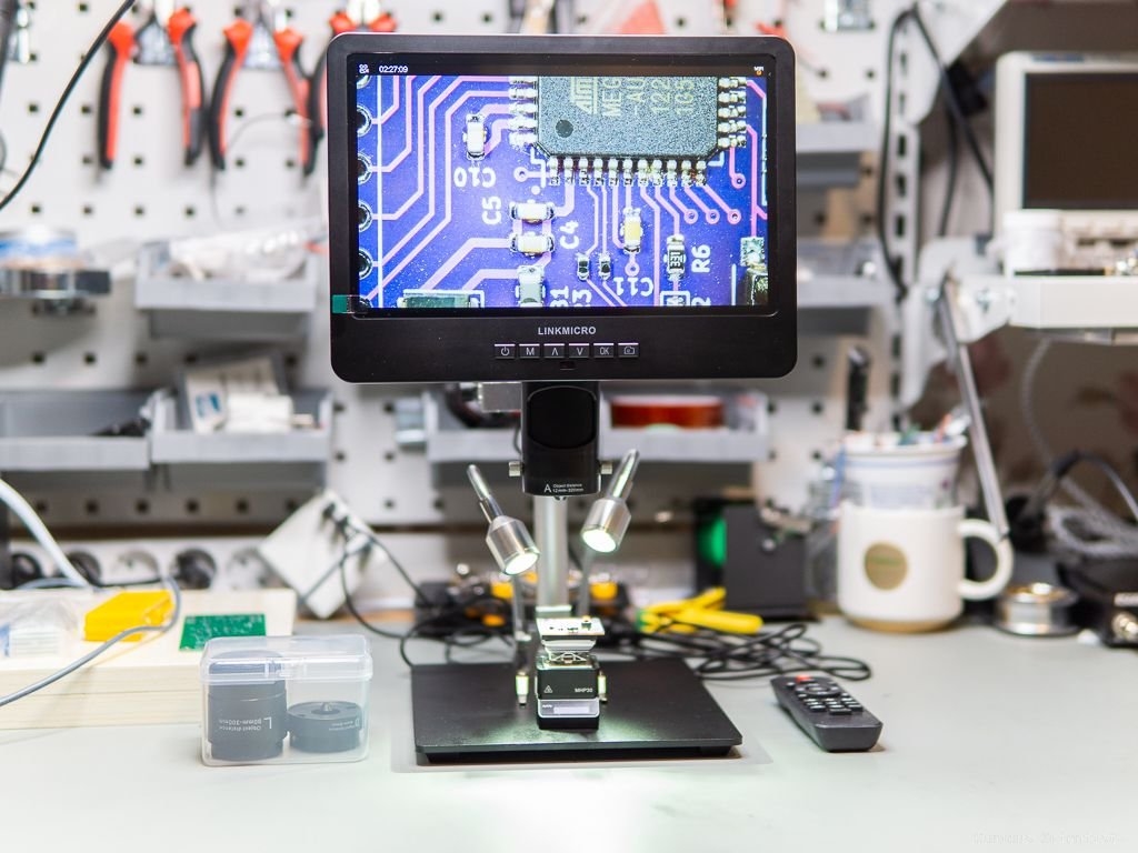
Next, validate stencil design through prototype testing. Apply solder paste using the step-down stencil on a sample board and inspect paste deposits before reflow. Adjust thickness or aperture sizes if deposits appear uneven. Post-reflow inspection should confirm joint formation aligns with IPC-A-610H criteria, focusing on fillet shape and wetting characteristics. Iterative testing minimizes defects before full-scale production.
During rework and repair, maintain documentation of stencil specifications used in original assembly. This information guides the selection of rework tools and solder paste types, ensuring compatibility. Use localized heating methods, as outlined in IPC-7711/7721C, to avoid thermal damage during component replacement. These steps preserve board integrity, leveraging the precision of step-down stencils for efficient outcomes.
Troubleshooting Common Issues with Step-Down Stencils
While step-down stencils offer significant advantages, challenges can arise during implementation. One common issue is paste release inconsistency in thinner stencil areas. If apertures are too small or stencil material lacks proper tension, paste may cling to the stencil rather than transfer to the board. Engineers should verify stencil fabrication meets tolerances specified in IPC-7525B, ensuring smooth release through polished aperture walls.
Another concern is misalignment during printing. Step-down regions must align precisely with PCB pads to avoid paste offset. Regular calibration of stencil printers, combined with optical inspection post-printing, helps detect and correct alignment issues early. If rework reveals recurring joint defects, revisit stencil design to confirm thickness variations match component needs, preventing systemic assembly errors.
Finally, wear and tear on step-down stencils can degrade performance over time. Routine cleaning and inspection prevent paste buildup, which alters deposit volumes. Adhering to maintenance protocols extends stencil life, sustaining solder joint quality across production runs. These troubleshooting steps ensure step-down stencils consistently support reliable SMT assembly and rework processes.
Conclusion
Step-down stencils represent a powerful solution for enhancing PCB rework and repair efficiency while bolstering solder joint quality in SMT assembly. By tailoring solder paste deposition to component-specific needs, these stencils minimize defects during initial assembly, simplifying subsequent rework tasks. Their impact on reliability ensures boards meet stringent performance demands in critical applications. Electrical engineers can leverage step-down stencil designs by following industry standards and best practices, achieving consistent outcomes in complex assembly environments. Through precise implementation and troubleshooting, this approach remains a cornerstone of modern PCB production, addressing the evolving challenges of high-density designs.
FAQs
Q1: How does a step-down stencil improve PCB rework efficiency?
A1: A step-down stencil enhances PCB rework by ensuring uniform solder paste application during initial assembly. This reduces defects like bridging or insufficient solder, making component removal cleaner and faster. With consistent joints, desoldering requires less heat, minimizing board damage. Standards like IPC-7711/7721C emphasize original assembly quality, which step-down stencils support effectively for streamlined rework.
Q2: What role does a step-down stencil play in solder joint quality?
A2: Step-down stencils optimize solder joint quality by controlling paste volume based on component size. Thinner areas prevent excess paste on fine-pitch parts, while thicker zones ensure adequate solder for larger components. This balance avoids defects, aligning with IPC-A-610H criteria for joint integrity, resulting in stronger, more reliable connections during SMT assembly.
Q3: Can step-down stencils enhance SMT assembly reliability?
A3: Yes, step-down stencils boost SMT assembly reliability by reducing solder-related defects. Precise paste deposition minimizes issues like voids or bridging, ensuring joints withstand thermal and mechanical stress. Following guidelines in IPC-7525B for stencil design, engineers achieve consistent results, leading to boards that perform reliably over time in demanding conditions.
Q4: What challenges might arise when using step-down stencils for PCB repair?
A4: Challenges with step-down stencils during PCB repair include paste release issues in thinner areas or misalignment during printing. These can affect initial joint quality, complicating repairs. Regular stencil maintenance and adherence to IPC-7525B tolerances help mitigate risks, ensuring repairs align with original assembly standards for optimal outcomes.
References
IPC-7525B — Stencil Design Guidelines. IPC, 2012.
IPC-A-610H — Acceptability of Electronic Assemblies. IPC, 2021.
IPC-7711/7721C — Rework, Modification and Repair of Electronic Assemblies. IPC, 2017.


