In the fast-paced world of PCB assembly, precision and efficiency are everything. If you're an electrical engineer looking to optimize the solder paste process in the manufacturing process, you might have heard about step-down stencils. So, why are engineers increasingly adopting this technology? Step-down stencils offer tailored control over solder paste volume, addressing the challenges of mixed component sizes on a single board, reducing defects, and improving overall assembly quality. In this blog, we’ll dive deep into the step-down stencil benefits, their role in PCB assembly, and why they are becoming a go-to solution for modern manufacturing.
What Are Step-Down Stencils and How Do They Work?
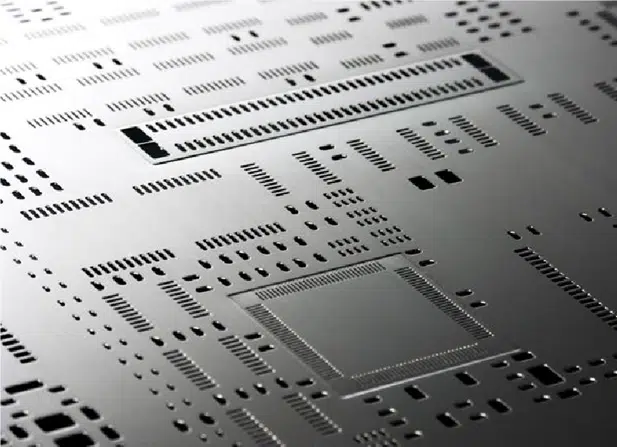
Step-down stencils are a specialized type of stencil used in the solder paste process during PCB assembly. Unlike standard stencils that have a uniform thickness, step-down stencils feature varying thicknesses across different areas of the stencil. These variations, or "steps," are created through advanced manufacturing techniques like chemical etching or laser cutting, allowing precise control over the amount of solder paste deposited on specific pads of a printed circuit board (PCB).
In a typical manufacturing process, a SMT stencil is placed over the PCB, and solder paste is applied through apertures (holes) in the stencil. The thickness of the stencil directly affects how much paste is deposited. With step-down stencils, thinner areas (step-down regions) deposit less paste, ideal for small components like 0402 resistors or fine-pitch ICs, while thicker areas allow more paste for larger components such as connectors or power devices. This customization ensures that each component gets the exact amount of solder paste needed for a reliable connection, minimizing issues like bridging or insufficient solder joints.
The Role of Stencil Use in PCB Assembly
Before diving deeper into step-down stencil benefits, let’s explore the broader importance of stencil use in PCB assembly. Stencils are critical tools in surface mount technology (SMT), where components are mounted directly onto the surface of a PCB. The stencil ensures that solder paste is applied accurately to the pads where components will be placed. Without a stencil, achieving uniform paste application across hundreds or thousands of pads would be nearly impossible, leading to inconsistent soldering and potential defects.
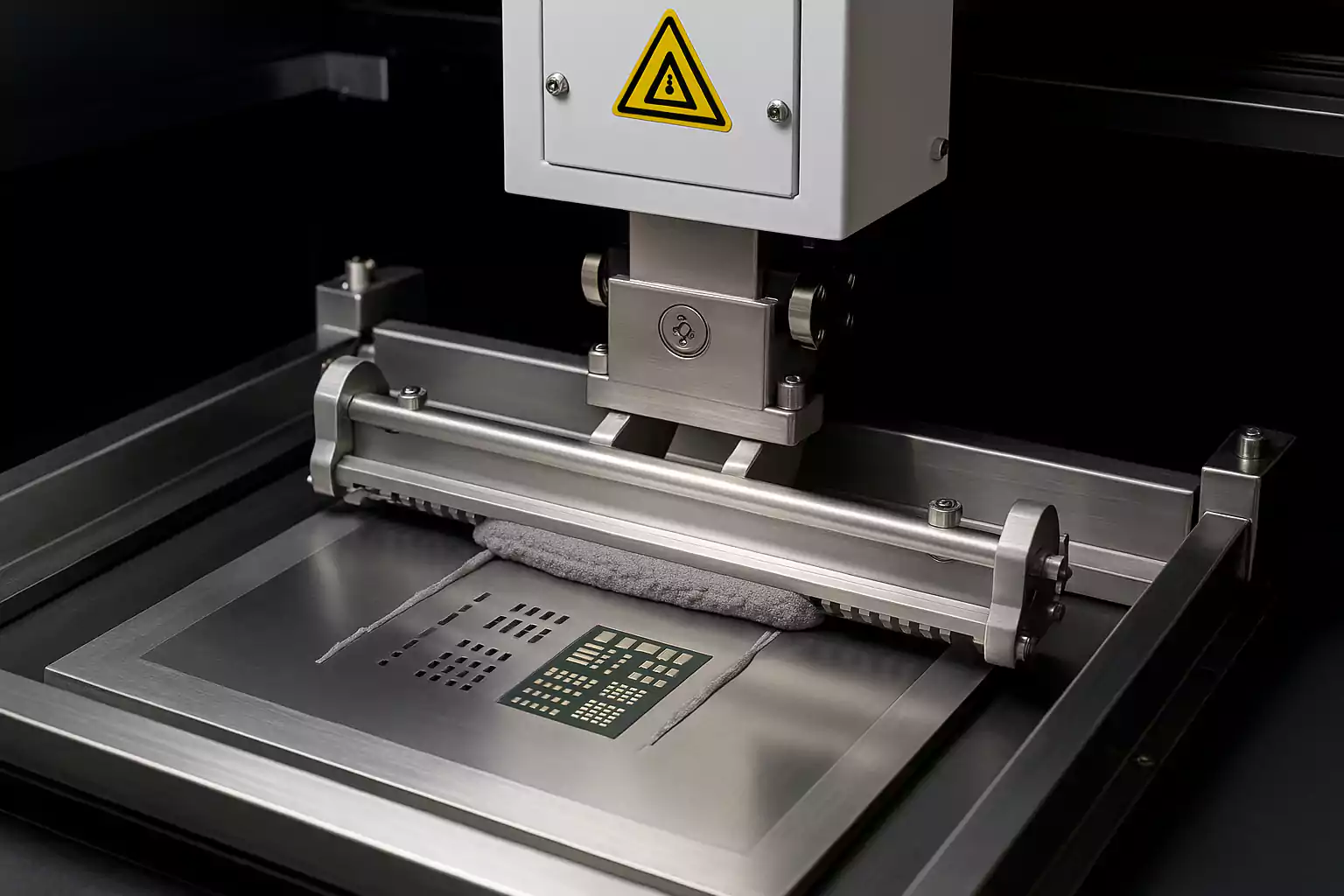
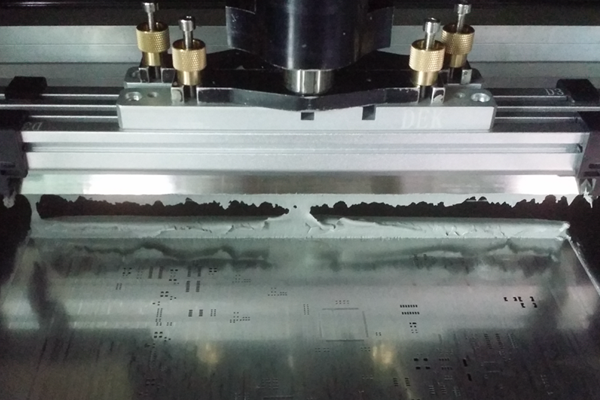
In a standard manufacturing process, stencils are typically made from stainless steel, with laser-cut openings that match the PCB layout. The solder paste is pushed through these openings using a squeegee, creating a precise pattern of paste deposits. After paste application, components are placed on the board, and the assembly undergoes reflow soldering, where the paste melts and forms electrical connections. The quality of this initial paste application often determines the success of the entire assembly process, making stencil design and material critical factors.
Why Step-Down Stencils Are Gaining Traction
Modern PCBs often feature a mix of component sizes and types, from tiny chip resistors to large power modules. A one-size-fits-all approach to stencil thickness doesn’t work in these scenarios. This is where step-down stencils shine. Here are some key reasons why engineers are moving toward this technology in the manufacturing process of PCB assembly.
1. Precise Control Over Solder Paste Volume
One of the standout step-down stencil benefits is the ability to control solder paste volume with pinpoint accuracy. Small components, like 0201 capacitors, require as little as 0.002 cubic millimeters of paste to avoid bridging, while larger components might need up to 0.01 cubic millimeters or more for a strong joint. A step-down stencil can have a thickness of 0.08 mm in areas for fine-pitch components and 0.15 mm in areas for larger parts, ensuring each pad gets the optimal paste volume. This reduces defects and improves first-pass yield rates in manufacturing, often by as much as 15-20% compared to standard stencils.
2. Reduced Defects in Mixed-Technology Boards
Mixed-technology boards, which combine small and large components, are common in applications like IoT devices, automotive electronics, and telecommunications equipment. Using a standard stencil on such boards often leads to over-pasting on small pads or under-pasting on larger ones. Step-down stencils address this by tailoring paste deposits to each component type, significantly lowering the risk of tombstoning, bridging, or insufficient solder. Studies in SMT processes have shown defect rates dropping from 5% to below 1% when using stepped stencils on complex boards.
3. Cost-Effective for High-Volume Production
While step-down stencils may have a higher upfront cost due to their complex design, they save money in the long run, especially in high-volume production. By reducing defects and rework, manufacturers can achieve better throughput and lower labor costs. For example, a production run of 10,000 boards with a 2% defect rate reduction can save thousands of dollars in rework and scrap costs. This makes step-down stencils a smart investment for engineers focused on scalability and efficiency in the manufacturing process.
4. Compatibility with Fine-Pitch and High-Density Designs
As PCB designs trend toward higher density and finer pitch—think 0.4 mm or even 0.3 mm spacing for ICs—standard stencils struggle to deliver consistent results. Step-down stencils, with their thinner regions, allow for finer control in these tight spaces, ensuring paste doesn’t overflow and cause shorts. This is critical for applications like mobile devices or wearable tech, where space is at a premium, and reliability is non-negotiable.
How Step-Down Stencils Fit into the Solder Paste Process
The solder paste process is the heart of SMT assembly, and step-down stencils play a pivotal role in ensuring its success. Let’s walk through how they integrate into this workflow and why they outperform standard options.
In the first step of the solder paste process, the stencil is aligned over the PCB using fiducial marks or automated vision systems for precision. With a step-down stencil, this alignment must account for the varying thicknesses, but modern stencil printers handle this seamlessly with adjustable pressure settings. Solder paste is then applied using a squeegee, and the stepped design ensures that each area of the board receives the appropriate paste thickness—thinner deposits for small pads and thicker for larger ones.
After paste application, the board moves to component placement and reflow soldering. The tailored paste volumes from a step-down stencil result in more uniform heating and cooling during reflow, reducing thermal stress on components. This leads to stronger solder joints and fewer failures during testing. For instance, boards assembled with step-down stencils often show a 10-15% improvement in joint reliability under thermal cycling tests compared to those using uniform stencils.
Challenges and Considerations with Step-Down Stencils
While the step-down stencil benefits are clear, there are some challenges engineers should keep in mind when integrating this technology into their manufacturing process.
First, designing a step-down stencil requires detailed knowledge of the PCB layout and component requirements. Engineers must work closely with stencil manufacturers to specify the exact thicknesses needed for different areas, often down to 0.02 mm precision. This adds a layer of complexity to the design phase, but modern CAD tools and simulation software can streamline this process.
Second, step-down stencils can be more prone to wear in thinner areas, especially under high-volume production. Regular inspection and cleaning are essential to maintain performance. Using high-quality materials like stainless steel with a hardness rating of at least 400 HV (Vickers Hardness) can extend stencil life by up to 30%, even in demanding environments.
Lastly, not all stencil printers are optimized for stepped designs. Older equipment may struggle with uneven squeegee pressure, leading to inconsistent paste deposits. Upgrading to a modern printer with programmable settings can mitigate this issue, ensuring the full benefits of step-down technology are realized.
Practical Tips for Implementing Step-Down Stencils
For electrical engineers new to step-down stencils, here are some actionable tips to maximize their effectiveness in PCB assembly.
- Collaborate Early: Work with your stencil provider during the design phase to map out step regions based on component datasheets and paste volume requirements. Aim for a thickness variation of no more than 0.05 mm between steps to maintain printing consistency.
- Test Small Batches: Before scaling to full production, run a small batch of boards with the step-down stencil. Use solder paste inspection (SPI) tools to verify deposit volumes and adjust stencil design if needed.
- Monitor Wear: Set a schedule for stencil inspection, especially after every 5,000 prints, to check for deformation in thinner areas. Replace stencils showing signs of wear to avoid quality issues.
- Optimize Printer Settings: Adjust squeegee speed and pressure based on the stencil’s stepped profile. A slower speed (around 20-30 mm/s) often works best for complex designs to ensure even paste distribution.
Future Trends: Where Step-Down Stencil Technology Is Heading
The adoption of step-down stencils is just the beginning. As PCB assembly continues to evolve, several trends are shaping the future of this technology. Miniaturization is pushing stencil designs toward even finer steps, with some manufacturers experimenting with thicknesses as low as 0.06 mm for ultra-fine-pitch components. Additionally, advancements in laser etching are making it easier and more cost-effective to produce complex stepped patterns, broadening access to this technology.
Another exciting development is the integration of step-down stencils with automated stencil printers equipped with real-time feedback systems. These systems can adjust printing parameters on the fly, compensating for stencil wear or paste viscosity changes, further enhancing reliability in the solder paste process. For engineers, staying ahead of these trends means better tools to tackle the challenges of next-generation electronics.
Conclusion: Why Step-Down Stencils Are a Game-Changer
In the world of PCB assembly, precision is paramount, and step-down stencils are proving to be a game-changer for electrical engineers. With benefits like tailored solder paste control, reduced defects, and compatibility with high-density designs, this technology addresses the unique challenges of modern manufacturing processes. By understanding the role of stencil use and leveraging the advantages of step-down designs, engineers can achieve higher quality, lower costs, and greater efficiency in their projects.
Whether you’re working on IoT devices, automotive systems, or consumer electronics, incorporating step-down stencils into your solder paste process can elevate your assembly outcomes. As the industry moves toward more complex and compact designs, adopting this technology isn’t just an option—it’s becoming a necessity for staying competitive. With the right approach and tools, step-down stencils can transform the way you build reliable, high-performance PCBs.


