Introduction
Modern printed circuit boards often feature components with varying heights, from tiny 01005 resistors to tall QFNs or inductors. This mix creates challenges during surface mount technology assembly, particularly in solder paste printing. Excess solder paste under tall components can lead to bridging, shorts, or reflow issues, while insufficient paste elsewhere causes weak joints. Step stencils address these problems by allowing precise control over paste volume across the board. Engineers rely on this technology to achieve reliable assembly yields in high-density designs. Understanding step stencil design proves essential for troubleshooting mixed-height assemblies.

What Are Step Stencils and Why Do They Matter?
Step stencils, also known as multi-level stencils, feature areas of different thicknesses within the same stencil frame. Thinner sections sit over tall components to deposit less solder paste, while standard thickness areas handle fine-pitch parts needing more volume. This design prevents the common issue of paste buildup that occurs with uniform stencils on mixed-technology boards. In practice, step stencils enable single-pass printing, saving time compared to multiple prints or manual adjustments. Their relevance grows with the trend toward miniaturized electronics packed with diverse component types. For electric engineers, mastering multi-level stencil benefits directly impacts assembly quality and production efficiency.
Without step stencils, assemblers face higher defect rates from inconsistent solder joints. Tall components like capacitors or connectors displace excess paste during placement, leading to bridging under neighboring parts. Step stencils optimize solder paste for different components by tailoring deposition heights precisely. Industry adoption has surged as board densities increase, making them a standard tool in SMT lines. Engineers troubleshooting print defects often trace issues back to improper volume control.
The Technical Principles Behind Step Stencils
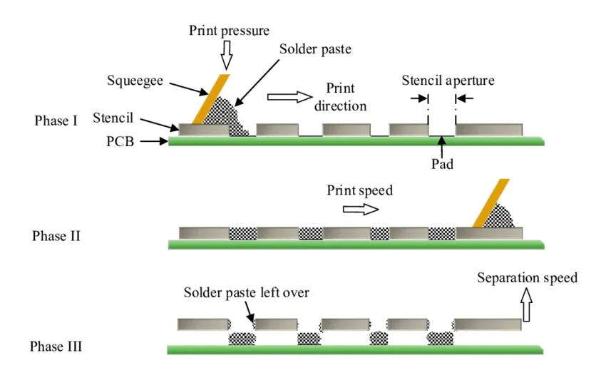
Step stencils work by varying the foil thickness, typically through stepped regions created during manufacturing. The thinner step reduces the aperture depth, limiting solder paste transfer to about half or less in those areas. This controlled volume ensures that after component placement and reflow, the solder joint height matches the component lead coplanarity. Solder paste rheology plays a key role; the paste must release cleanly from thinner walls without starving adjacent thicker areas. Engineers design steps based on component standoff heights and pad sizes to maintain aspect ratios for good release.
Key to performance is the transition zone between levels, where keep-out rules prevent paste smearing. IPC-7525 guidelines specify minimum distances around steps to avoid defects like bridging or insufficient fill. The thinner area's sidewall finish affects paste scoop-up during printing, so polished surfaces enhance transfer efficiency. Thermal expansion differences between levels must align with PCB tolerances for consistent gasketing. In troubleshooting, engineers measure paste height post-print using profilometers to validate design assumptions.
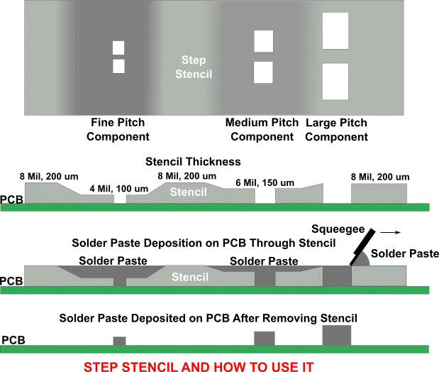
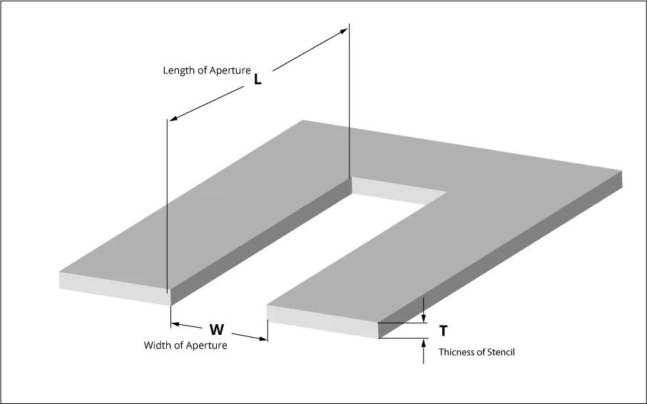
Paste volume control hinges on stencil thickness relative to aperture size. Standard stencils use 125 to 150 micron foils for most fine-pitch parts, but steps drop to 75 to 100 microns over protrusions. This adjustment compensates for component height differences up to several hundred microns. During squeegee passage, pressure and speed influence fill in stepped areas, requiring process optimization. Multi-level stencil benefits shine in high-mix production, where one stencil handles diverse packages without changeovers.
Step Stencil Design Considerations
Effective step stencil design starts with analyzing the bill of materials for height variations. Engineers map tall components and define step locations, ensuring no overlap with fine-pitch arrays. Aperture shapes in thin areas often use trapezoidal or U-forms to improve paste release per IPC-7525 recommendations. Home plating or etching adds to sidewall quality, reducing tackiness that causes defects. Designers simulate print volumes using software to predict joint formation before fabrication.
Optimizing solder paste for different components involves calculating transfer efficiency targets. For tall QFNs, reduce volume by 40 to 60 percent via thinner stencils to avoid fillet excess. Conversely, micro BGAs need full volume for reliable balls. Step heights typically range in increments matching common component stands-offs, with transitions smoothed to minimize squeegee drag. Troubleshooting poor release often reveals undersized apertures or rough walls in the design phase.
Keep-out zones around steps prevent paste bridging during printing. Guidelines recommend scaling distance with step depth to maintain clean separation. Board warpage influences gasket pressure, so flatness checks precede design finalization. Engineers iterate designs based on SPI data from trial runs.
Step Stencil Manufacturing Processes
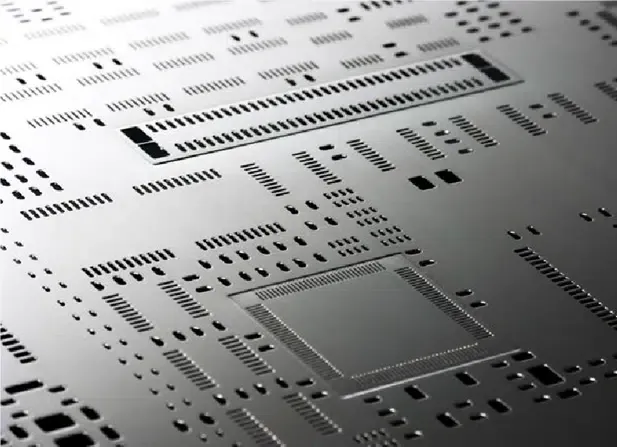
Step stencil manufacturing combines laser cutting, electroforming, and welding for precision. Base foils start as stainless steel sheets, etched or YAG laser-cut for apertures. Steps form by framing thinner foils and welding them to the thicker base, often using nano-coating for release. Etch-back techniques create recessed areas without multi-foils for simpler designs. Quality checks include profilometry for thickness uniformity and optical inspection for wall angles.
Laser-based methods dominate for step stencil manufacturing due to tight tolerances on step edges. Post-processing like polishing ensures smooth transitions, critical for paste flow. Manufacturers stress-relieve foils to prevent warping under print pressure. Frame materials match for thermal stability during high-volume runs. Engineers specify tolerances like plus or minus 5 microns on thicknesses to meet J-STD-001 assembly criteria.
Variations include hybrid stencils with electroformed steps for ultra-fine features. Coating options like nano-titanium enhance cleanability and longevity. Incoming inspection verifies step coplanarity to avoid print skips.
Practical Best Practices and Troubleshooting
Implement step stencils by verifying PCB flatness first, as warpage exceeds 0.75 percent causes gasket leaks. Align fiducials precisely for sub-25 micron overlay. Use type 4 or 5 paste for better flow in thin areas, adjusting viscosity for humidity. Print speeds slow to 20 to 40 mm/sec over steps to aid fill. Clean stencils every 5 to 10 prints with optimized wipe sequences.
Troubleshooting starts with solder paste inspection post-print. Low volume in thick areas signals poor squeegee pressure; high in thin areas points to step misalignment. Bridging near transitions often traces to inadequate keep-out or rough walls. Reflow defects like head-in-pillow link back to volume imbalance, confirmed by cross-section analysis. Iterate by tweaking step heights or apertures based on data.
For high-reliability boards, validate against IPC-A-610 class criteria. Process windows narrow with finer pitches, so DOE on parameters proves robust. Multi-level stencil benefits extend to yield gains of 20 percent or more in mixed assemblies.
Common Pitfalls and Case Insights
In one scenario, a board with adjacent tall inductors and 0201 resistors suffered chronic bridging. The fix involved widening keep-outs and thinning steps further, restoring yields. Another case saw tombstoning from uneven reflow, resolved by balancing paste volumes precisely. These highlight the need for holistic design review.
Engineers often overlook stencil tensioning, leading to flex over steps. Proper fixturing maintains planarity. Long-term, track stencil wear; steps degrade faster, requiring rotation.
Conclusion
Step stencils unlock reliable assembly for PCBs with mixed component heights through targeted solder paste volume control. Their design and manufacturing enable precise optimization across diverse packages. Electric engineers benefit from higher yields and fewer reflow headaches by following best practices. Integrating IPC guidelines ensures compliance and performance. As densities rise, step stencils remain indispensable for efficient SMT processes.
FAQs
Q1: What is step stencil design and how does it improve PCB assembly?
A1: Step stencil design incorporates varying thicknesses to deposit appropriate solder paste volumes for components of different heights. This prevents excess paste under tall parts, reducing bridging and improving joint quality. Engineers follow IPC-7525 for aperture rules and keep-outs, enabling single-pass printing on mixed boards. The result is higher yields and compliance with assembly standards.
Q2: What are the multi-level stencil benefits for solder paste volume control?
A2: Multi-level stencils provide precise solder paste volume control by thinning areas over protrusions, avoiding reflow defects like shorts. They support fine-pitch and large components on one board, cutting process steps. Troubleshooting focuses on transition zones for clean prints. Overall, they boost efficiency in high-mix production.
Q3: How does optimizing solder paste for different components work with step stencils?
A3: Optimizing solder paste for different components uses thinner stencil sections to limit volume on tall parts while maintaining full deposition elsewhere. This matches paste height to standoffs, ensuring reliable joints post-reflow. Process tweaks like squeegee speed fine-tune transfer. Validation via SPI confirms balance.
Q4: What role does step stencil manufacturing play in assembly success?
A4: Step stencil manufacturing employs laser cutting and welding for accurate multi-thickness foils, with coatings for paste release. Precision in steps and walls directly affects print quality. Engineers specify tolerances to meet J-STD-001 criteria, minimizing defects. Regular maintenance extends usability.
References
IPC-7525C — Stencil Design Guidelines. IPC, 2021
IPC J-STD-001 — Requirements for Soldered Electrical and Electronic Assemblies. IPC, 2017
IPC-A-610 — Acceptability of Electronic Assemblies. IPC, 2017