Introduction
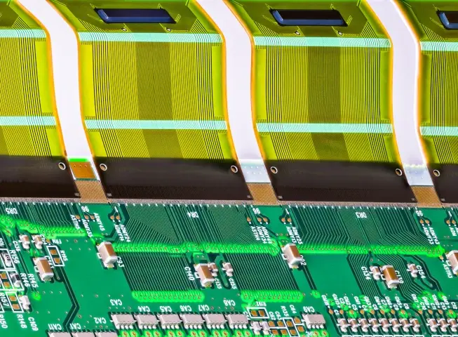
Assembling flex and rigid-flex printed circuit boards presents unique challenges due to their inherent flexibility and varying thicknesses. Traditional flat stencils often fail to deliver consistent solder paste deposition on these substrates, leading to defects such as insufficient paste volume, bridging, or poor release in warped areas. Step-up stencils address these issues by providing multi-level thickness variations that compensate for surface unevenness and component-specific paste requirements. This approach ensures reliable flexible joints, critical for applications in wearables, medical devices, and automotive electronics where movement and thermal cycling stress solder connections. Engineers must prioritize precise stencil design to minimize joint fatigue and fractures common in flexible assembly. By integrating step-up features, manufacturers achieve higher yields and long-term reliability without compromising on miniaturization trends.

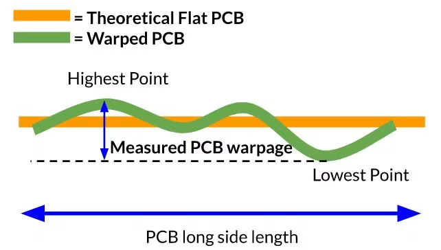
Flex PCBs warp under heat, handling, or moisture, exacerbating stencil contact problems during printing. Rigid-flex boards compound this with abrupt transitions between rigid and flexible sections, creating coplanarity deviations that disrupt uniform paste transfer. Step-up stencil flexible circuits solutions enable targeted paste volumes, particularly beneficial for mixed fine-pitch and larger components on uneven surfaces. These stencils promote consistent reflow outcomes, reducing voids and improving mechanical integrity of solder joints.
Related Reading: Optimizing Solder Paste Application with Step Up Stencils
What Are Step-Up Stencils and Why They Matter for Flex and Rigid-Flex PCBs
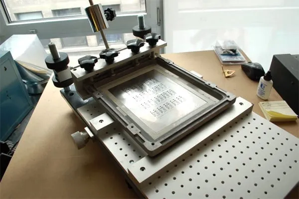
Step-up stencils are advanced SMT stencils featuring localized thicker regions to deposit greater solder paste volumes in specific board areas. Unlike uniform-thickness stencils, they incorporate raised steps, typically created via laser cutting or etching, allowing precise control over paste height for components needing extra material, such as inductors or connectors on flex sections. This design is particularly vital for flex PCB stencil applications where substrate thinness leads to sagging or bowing during assembly. Rigid flex stencil requirements demand similar adaptations to handle height differences between rigid FR4 sections and polyimide flex zones.
As detailed in our comprehensive guide to designing and manufacturing flex and rigid-flex PCBs, the relevance of specialized tooling stems from flex PCB vulnerabilities to dimensional instability. Thin substrates like polyimide absorb moisture, causing warpage that misaligns the stencil and results in starved joints or excess paste buildup. Step-up configurations mitigate these by enabling more paste in low-lying flex areas, fostering reliable flexible joints that withstand bending cycles. Industry guidelines in IPC-7525 outline step stencil parameters to optimize print quality across varied topographies.
Without such solutions, flexible assembly yields suffer from inconsistent wetting and intermetallic formation issues. Procurement teams benefit from reduced rework, while designers gain confidence in high-density layouts. Ultimately, step-up stencils bridge the gap between rigid board processes and the demands of dynamic substrates.
Technical Principles of Step-Up Stencils in Flexible Assembly
The core mechanism of step-up stencils lies in their multi-level foil structure, where step heights adjust paste extrusion based on aperture design and board topography. During printing, the squeegee blade sweeps across the stencil, forcing paste into apertures; thicker step-up zones yield taller deposits ideal for compensating flex warpage-induced gaps. This ensures the paste bridges minor surface deviations, promoting uniform standoff heights post-reflow for robust solder fillets.
Flex and rigid-flex PCBs exhibit coplanarity challenges due to material properties: polyimide flex layers contract under reflow heat, while rigid sections remain stable, creating up to localized height variances. Step-up stencils counteract this by increasing paste volume in recessed flex regions, enhancing joint fillet formation and reducing head-in-pillow defects. Paste release improves with electropolished surfaces on these stencils, minimizing stringing on delicate substrates.
IPC-7525 provides foundational rules for step dimensions, recommending minimum land widths and step transitions to avoid bridging. In practice, the step-up feature aligns with the need for higher paste-to-aperture ratios in flexible circuits, where movement risks displacing deposits. Thermal expansion mismatches further underscore the need for tailored volumes to prevent cracks at flex-to-rigid interfaces.
Practical Solutions and Best Practices for Reliable Solder Joints
Implement step-up stencils by first analyzing board layout for warpage-prone zones, designing steps over flex areas requiring extra paste. Collaborate with fabricators for laser-cut stainless steel foils, typically thinner overall for flex PCB stencil compatibility to enhance conformity. Pair with rigid carrier jigs or vacuum fixtures to flatten the substrate during printing, ensuring consistent stencil-to-board gapping.
Optimize solder paste selection with finer particle sizes for high-aspect-ratio apertures common in flexible assembly. Adjust printer parameters like reduced squeegee pressure and moderate speeds to accommodate substrate give without smearing. Clean stencils frequently to prevent paste buildup, which exacerbates defects on uneven surfaces.
Post-print verification using SPI or 3D inspection confirms volume uniformity, targeting defect rates aligned with IPC-610 acceptability criteria for electronic assemblies. For rigid-flex, extend steps across transition zones to balance paste across sections. These practices yield reliable flexible joints capable of enduring cyclic flexing.
Incorporate design aids like teardrop pads to bolster joint strength against fatigue. Pre-bake boards to expel moisture, minimizing popcorn effects that warp flex layers further.
Related Reading: Implementing DFA in Flex and Rigid Flex PCB Design
Troubleshooting Common Issues with Flex and Rigid-Flex Stencil Printing
Warpage tops the list of flex PCB stencil challenges, manifesting as insufficient paste transfer in bowed regions. Solution: Employ step-up features combined with pin-aligned carriers to force planarity; verify with shadow moiré analysis pre-assembly. Bridging often occurs at fine-pitch areas due to paste slumping on flex; counter with optimized aperture walls and nano-coatings for superior release.
Insufficient solder volume in flex zones leads to open joints; step-up stencils directly resolve this by boosting deposits selectively. Alignment shifts from handling demand vision-corrected printers and fiducials near bends. For rigid-flex, height mismatches cause gapping over rigid sections; step-down complements in hybrid designs, but step-up excels for paste augmentation.
Reflow defects like voids trace to uneven paste; troubleshoot via X-ray and correlate to print inspections. Consistent application of these fixes, per industry-aligned processes, elevates overall assembly reliability.
Conclusion
Step-up stencil solutions revolutionize flex PCB stencil and rigid flex stencil processes by delivering precise paste control amid warpage and topography hurdles. These multi-level designs ensure reliable flexible joints through enhanced volume deposition and compatibility with support fixtures. Adhering to IPC-6013 qualification specs for flex boards guarantees performance under stress. Engineers achieve superior yields, fewer defects, and durable assemblies for demanding applications. Integrating best practices positions flexible assembly as a reliable production staple.
FAQs
Q1: What makes step-up stencils essential for flex PCB stencil printing?
A1: Step-up stencils provide varying thicknesses to deposit more solder paste in warped or recessed flex areas, overcoming uneven surfaces that plague standard stencils. This results in consistent transfer and reliable flexible joints despite substrate movement. Pairing with jigs flattens boards for optimal contact, aligning with practical flexible assembly needs.
Q2: How do rigid flex stencil designs handle section height differences?
A2: Rigid-flex boards feature rigid sections thicker than flex zones, causing coplanarity issues during printing. Step-up configurations increase paste in lower flex regions for uniform joints, while fixtures maintain stability. This targeted approach minimizes voids and bridges for robust performance.
Q3: What best practices improve outcomes with step-up stencil flexible circuits?
A3: Use thinner foils, fine-particle paste, and controlled printing parameters alongside rigid carriers. Regular cleaning and SPI inspection verify deposition quality. These steps ensure reliable solder joints in high-flex applications without excessive rework.
Q4: Can step-up stencils reduce solder joint fatigue in flexible assembly?
A4: Yes, by enabling optimal paste volumes that form strong fillets resistant to bending stresses. Proper design per stencil guidelines prevents underfill, enhancing mechanical integrity across cycles. Inspection confirms compliance with joint acceptability standards.
References
IPC-7525C — Stencil Design Guidelines. IPC.
IPC-6013D — Qualification and Performance Specification for Flexible and Rigid-Flex Printed Boards. IPC.
IPC-610G — Acceptability of Electronic Assemblies. IPC.