Introduction
In PCB assembly processes, achieving precise solder paste deposition is essential for reliable solder joints and minimizing defects. Modern circuit boards often feature a mix of fine-pitch components and larger parts with varying standoff heights, making uniform stencil thickness inadequate. Step-up stencils and step-down stencils represent advanced stencil types that address these challenges by allowing controlled solder paste volume across different areas of the board. These variations enable engineers to optimize paste height and volume tailored to specific component requirements during surface mount technology operations. Understanding the differences between step-up and step-down stencils helps in selecting the right approach for complex assemblies, improving yield and reducing rework.
What Are Step-Up and Step-Down Stencils?
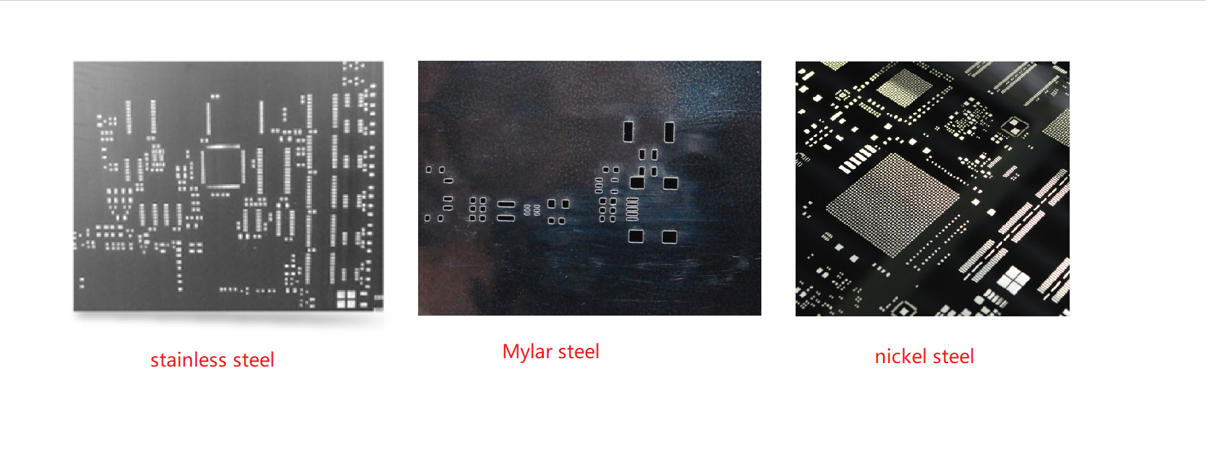
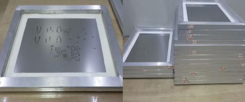
Stencils serve as the primary tool for applying solder paste onto PCB pads in a controlled manner before component placement. A standard stencil maintains uniform thickness across its surface, typically suited for boards with consistent component sizes. Step stencils, however, introduce thickness variations to handle mixed-technology boards where solder paste volume needs differ. A step-down stencil features areas thinned down from a thicker base, ideal for fine-pitch devices that require less paste to avoid bridging or tombstoning. Conversely, a step-up stencil builds up thickness in select regions from a thinner base, providing extra paste height for larger components or those needing mechanical strength.
These stencil types emerged as solutions to the limitations of flat stencils in high-density interconnects. IPC-7525B outlines guidelines for their design, emphasizing keep-out zones around steps to ensure clean printing. By modulating thickness, engineers can achieve solder paste volumes that align with component standoffs and pitch requirements without multiple printing passes.
Key Differences Between Step-Up and Step-Down Stencils
The primary distinction lies in their approach to thickness variation relative to the base stencil. In a step-down stencil, the majority of the stencil remains at a standard thickness, with localized reductions for small-pitch components, effectively lowering solder paste volume in those zones. This prevents excess paste that could lead to shorts during reflow. A step-up stencil reverses this: the base is thinner to accommodate fine-pitch areas, while raised sections deliver increased paste volume for bulky parts like connectors or inductors.
Manufacturing methods also differ slightly. Step-down areas are often created by etching away material, while step-up regions may involve additive processes like electroforming or laser welding thicker foils. Both require precise alignment to avoid printing artifacts, but step-up stencils demand greater care in adhesion and stability during printing. Solder paste volume control is more versatile with step-up designs for boards dominated by large components, whereas step-down excels in high-I/O fine-pitch scenarios.
From a practical standpoint, step-down stencils reduce the risk of paste bridging on dense pads, while step-up stencils ensure sufficient fillet height for mechanical reliability. IPC-7525B recommends specific design rules for step transitions to maintain aperture integrity.
Technical Principles Behind Step Stencils
Solder paste deposition volume is directly proportional to stencil thickness and aperture area. Uniform stencils deposit consistent heights, but component diversity necessitates variation. Step-down stencils lower thickness in fine-pitch zones, typically reducing paste height to improve release properties and minimize solder balls post-reflow. This aligns with the need for precise joints in micro-BGA or 01005 components where excess volume causes defects.
Step-up stencils increase thickness selectively, compensating for components with higher standoffs or pin-in-paste applications. The raised areas deposit taller paste bricks, promoting better wetting and joint strength without compromising fine-pitch regions. Printing dynamics play a role: squeegee pressure must be optimized to fill stepped apertures fully without smearing at transitions. Surface tension of the paste influences release from thinner walls in step-down areas, often requiring nano-coatings for better performance.
Design considerations include aspect ratios and area ratios per IPC-7525B, ensuring apertures release paste cleanly. Keep-out distances around steps prevent stencil flexing that could distort deposits. Thermal expansion during laser cutting or etching must match the frame material to avoid warpage.
Applications in PCB Assembly
Step-down stencils shine in high-density consumer electronics where fine-pitch ICs coexist with mid-sized passives. They control solder paste volume precisely, reducing defects like bridging by 20-30% in typical runs, though exact gains depend on process tuning. Automotive and telecom boards benefit from their ability to handle 0.3mm pitch without secondary printing.
Step-up stencils suit industrial controls or power supplies with large QFPs, relays, and edge connectors needing robust joints. Pin-in-paste techniques leverage the extra height for through-hole simulation in SMT lines. Hybrid boards with both fine and coarse elements, common in IoT devices, often combine both step types in a single stencil for streamlined assembly.
In double-sided PCBs, step stencils prevent paste smear from bottom-side reflow affecting top deposits. Their use extends to low-volume prototypes where flexibility trumps cost.
Best Practices for Implementation
Select stencil thickness based on the smallest pitch: thinner for ultra-fine, thicker base for step-down. Aperture reduction of 5-10% on pads improves volume control without altering land patterns. Validate designs via simulation software modeling paste flow before fabrication.
Printing parameters demand adjustment: slower speeds for step transitions, consistent pressure to avoid skips. Clean stencils frequently to prevent paste drying in pockets. Post-print inspection with SPI verifies volume uniformity across steps.
Per IPC J-STD-001, joints from stepped stencils must meet Class 2 or 3 criteria for voiding and fillet formation. Test reflow profiles to ensure collapse matches component heights.
Troubleshooting Common Issues
Insufficient paste in step-up areas often stems from poor squeegee contact; increase blade angle or pressure incrementally. Bridging in step-down zones indicates inadequate area ratios—increase keep-outs or refine apertures. Stencil damage at steps arises from misalignment; use fiducials for registration.
Warpage in additive step-up foils causes uneven deposits: opt for etched methods or stress-relief annealing. If paste release fails, apply release coatings and monitor humidity. Analyze defects with X-ray or cross-sectioning to correlate with stencil features.
Conclusion
Step-up and step-down stencils offer targeted solder paste volume control, essential for modern PCB assembly challenges. Step-down excels at fine-pitch precision, while step-up bolsters large-component reliability. By following IPC-7525B guidelines, engineers can integrate these stencil types effectively, enhancing yield and joint quality. Selecting the appropriate variant based on board complexity ensures optimal performance without excessive rework.
FAQs
Q1: What is the main advantage of a step-down stencil in PCB assembly?
A1: Step-down stencils reduce solder paste volume in fine-pitch areas, minimizing bridging and solder balls on dense components. This allows a thicker base for larger parts while optimizing deposits for micro-components, improving overall print yields. Per industry guidelines, they align with mixed-pitch requirements without multiple stencils.
Q2: When should I choose a step-up stencil over a standard one?
A2: Use step-up stencils for boards with components needing higher solder paste volume, like connectors or standoff-heavy parts. The raised areas provide extra height from a thin base suited to fine pitch elsewhere. This stencil type prevents insufficient fillets, enhancing mechanical strength in PCB assembly.
Q3: How do step-up and step-down stencils affect solder paste volume?
A3: Step-up stencils increase volume in select thicker zones for robust joints, while step-down stencils decrease it in thinner areas to avoid defects on small pads. Both control deposition precisely across stencil types, critical for mixed assemblies. Design per IPC-7525B ensures balanced performance.
Q4: Can step-up and step-down features be combined in one stencil?
A4: Yes, hybrid stencils with both step-up and step-down regions handle extreme component diversity effectively. This approach streamlines printing for complex boards, controlling solder paste volume optimally. Careful design prevents transition issues during PCB assembly.
References
IPC-7525B — Stencil Design Guidelines. IPC, 2011
IPC J-STD-001H — Requirements for Soldered Electrical and Electronic Assemblies. IPC, 2018


