Introduction
In the realm of printed circuit board (PCB) assembly, the interplay between PCB pad design and solder paste application plays a pivotal role in ensuring reliable electrical connections and structural integrity. For electrical engineers, understanding this relationship is essential to achieving high-quality solder joints that withstand operational stresses. Solder paste, a mixture of flux and metal particles, acts as the bonding agent during reflow soldering, while pad design dictates how effectively this paste forms a joint. Factors like pad area, shape, and solder paste volume directly influence outcomes. This article explores the technical nuances of PCB pad design, solder paste application, and their combined impact on assembly quality. By adhering to recognized industry standards, engineers can optimize designs for manufacturability and performance, reducing defects and enhancing product longevity.
What Is PCB Pad Design and Why It Matters
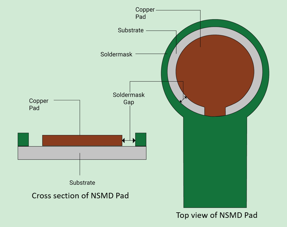
PCB pad design refers to the layout and geometry of conductive areas on a board where components are soldered. These pads serve as the interface between the component leads or terminations and the board's circuitry. A well-designed pad ensures proper solder paste application, facilitates heat transfer during reflow, and supports mechanical stability. Poor pad design, on the other hand, can lead to issues like insufficient wetting, tombstoning, or solder voids, all of which compromise connection reliability.
The significance of pad design extends beyond aesthetics to functional performance. Electrical engineers must consider pad dimensions, spacing, and alignment with component footprints to prevent assembly errors. Standards such as IPC-7351B provide guidelines for creating land patterns that match component specifications, ensuring compatibility with solder paste application processes. When pads are designed with precision, they accommodate the correct solder paste volume, minimize defects, and enhance the durability of the final product.
Technical Principles of PCB Pad Design and Solder Paste Interaction
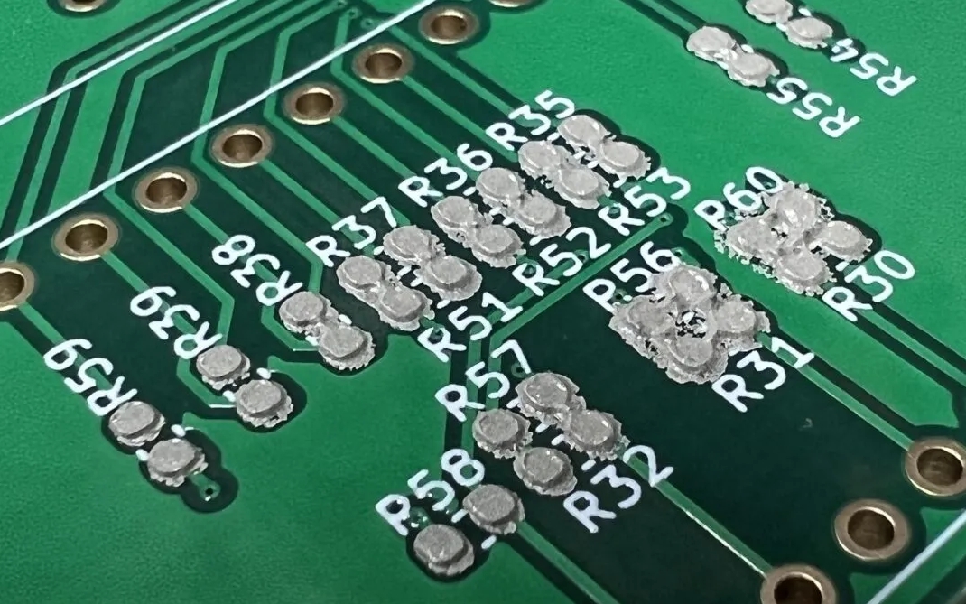
The relationship between PCB pad design and solder paste hinges on several technical factors, including pad area, shape, and the resulting solder paste volume and height. Pad area determines the amount of solder paste that can be applied, directly affecting the joint's strength and electrical conductivity. Larger pads may hold more paste, but excessive volume can cause bridging between adjacent pads, leading to shorts. Conversely, smaller pads with insufficient paste may result in weak joints prone to cracking under thermal or mechanical stress.
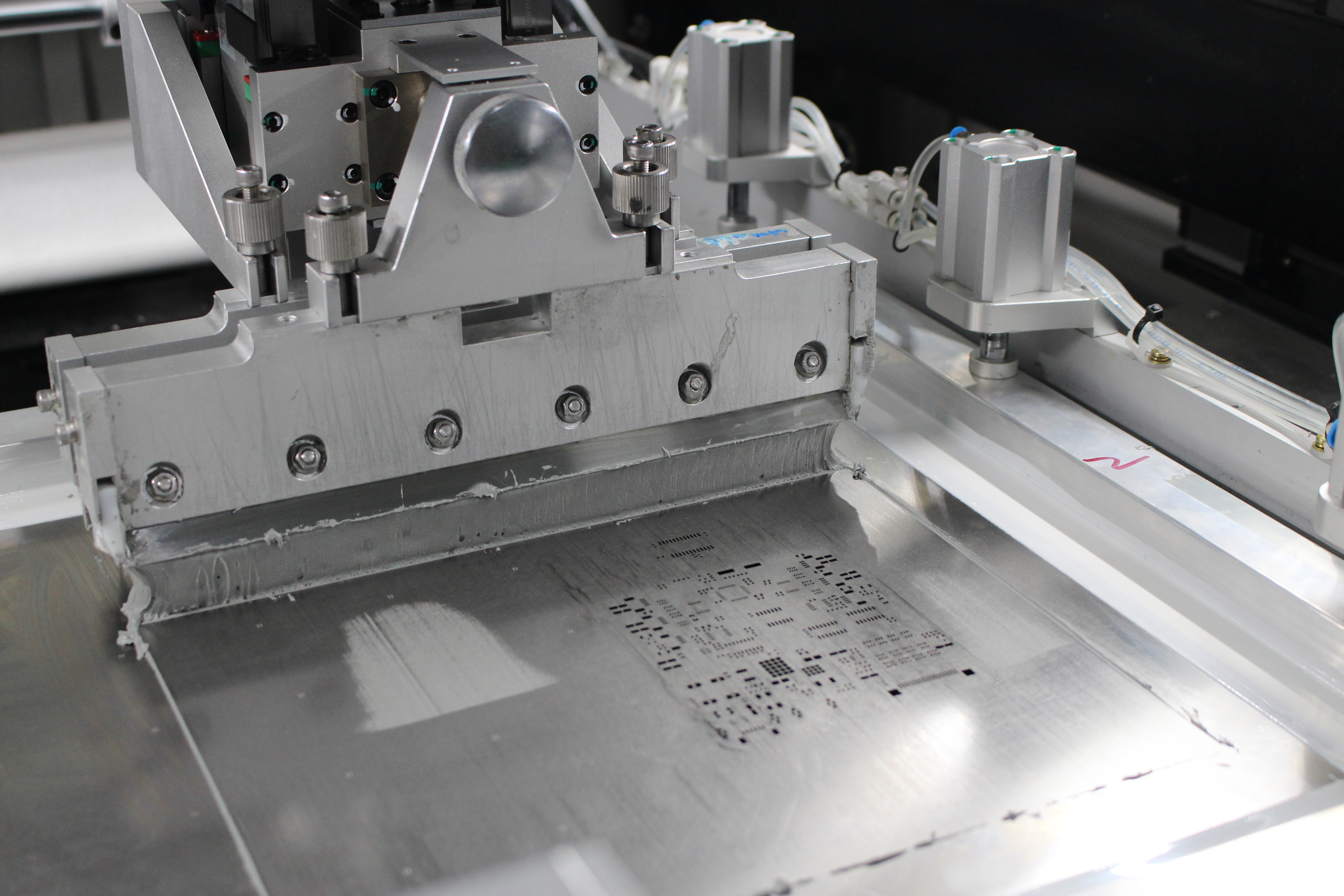
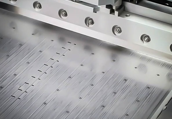
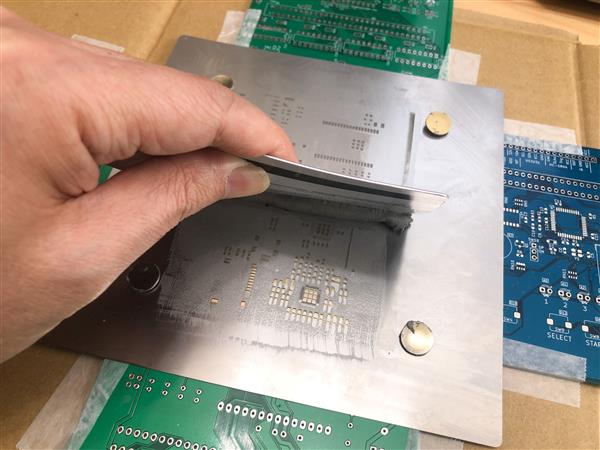
Solder paste height, influenced by stencil thickness and aperture design, also plays a critical role. If the height is too low, the paste may not form a proper fillet during reflow, reducing joint reliability. If too high, excess paste can squeeze out, risking defects. According to guidelines in IPC-7525B, stencil design must align with pad geometry to control solder paste deposition accurately. Engineers must balance these parameters to achieve consistent results.
Pad shape further impacts solder paste behavior. Rectangular pads, often used for surface-mount components, provide a uniform area for paste application, while circular pads may be preferred for through-hole components to aid in capillary action during soldering. The choice of shape influences how solder wets the pad and component lead, a process governed by surface tension and thermal dynamics during reflow.
Thermal considerations are equally important. Pads connected to large copper planes can act as heat sinks, drawing heat away from the solder joint and causing uneven melting of solder paste. IPC-2221B recommends thermal relief patterns in such cases to ensure uniform heating and prevent cold solder joints. Understanding these principles allows engineers to predict and mitigate potential issues during assembly.
Impact of Solder Paste Volume, Area, and Height on Assembly Quality
Solder paste volume is a critical parameter that must correspond to the pad area for optimal joint formation. Volume is typically controlled by the stencil aperture size and thickness, which dictate how much paste is deposited onto each pad. A mismatch between pad area and solder paste volume can lead to defects. For instance, excessive volume on a small pad can cause solder balls or bridging, while insufficient volume on a larger pad may result in incomplete wetting.
The area of the pad directly correlates with the required solder paste volume. Standards like IPC-J-STD-005A outline methods for calculating appropriate paste quantities based on pad dimensions and component requirements. Engineers must ensure that the stencil aperture matches the pad area to deposit a consistent layer of paste, avoiding over or under-application.
Height of the solder paste deposit, determined by stencil thickness, affects the final joint profile. A thicker stencil increases paste height, potentially leading to excess material that spreads during reflow. A thinner stencil reduces height, which may be insufficient for forming a robust joint. IPC-7525B provides detailed guidance on selecting stencil thickness based on component pitch and pad size to maintain the desired solder paste height.
Balancing these factors requires precise calculations and testing. For fine-pitch components, where pad areas are smaller, controlling solder paste volume and height becomes even more challenging. Engineers often rely on design rules from IPC-7351B to define pad dimensions and corresponding stencil apertures, ensuring compatibility with automated assembly processes.
Related Reading: Optimizing Solder Paste Application with Step Up Stencils
Best Practices for Optimizing PCB Pad Design and Solder Paste Application
Achieving reliable solder joints starts with adhering to established design and assembly guidelines. Electrical engineers can follow these best practices to optimize PCB pad design and solder paste application, minimizing defects and enhancing performance.
First, align pad dimensions with component specifications using standards like IPC-7351B. This ensures that the pad area is appropriate for the component footprint, providing a stable base for solder paste. Pay attention to pad spacing, especially for fine-pitch devices, to prevent bridging during reflow.
Second, design stencils with apertures that match pad geometry. According to IPC-7525B, aperture size should be slightly smaller than the pad to account for paste spread during printing. Select stencil thickness based on the required solder paste height, considering component type and assembly process.
Third, incorporate thermal relief patterns for pads connected to large copper areas, as recommended by IPC-2221B. This prevents heat dissipation issues that can affect solder paste melting and joint formation. Use simulation tools to predict thermal behavior during reflow and adjust pad design accordingly.
Fourth, verify solder paste volume through inspection methods outlined in IPC-J-STD-005A. Automated optical inspection systems can detect inconsistencies in paste deposition, allowing for immediate corrections before reflow. Adjust stencil design or printing parameters if volume deviations are observed.
Finally, maintain clean and controlled assembly environments to avoid contamination of solder paste. Flux residues or debris on pads can interfere with wetting, leading to poor joints. Following cleanliness guidelines from IPC-J-STD-001H ensures that solder paste application yields consistent results.
Related Reading: The Ultimate Guide to SMT Stencil Pad Design for Beginners
Troubleshooting Common Issues in Solder Paste and Pad Design Integration
Despite careful planning, issues can arise during solder paste application due to pad design mismatches or process variations. Electrical engineers must be prepared to identify and resolve these problems efficiently.
One common issue is solder bridging, often caused by excessive solder paste volume on closely spaced pads. Reducing stencil aperture size or adjusting paste viscosity can mitigate this, as suggested by IPC-7525B. Additionally, ensure pad spacing adheres to IPC-7351B guidelines for fine-pitch components.
Another frequent problem is insufficient wetting, where solder paste fails to bond properly with the pad or component lead. This can result from undersized pads or inadequate paste height. Review pad dimensions against component requirements and increase stencil thickness if necessary, following IPC-J-STD-005A recommendations.
Tombstoning, where one end of a component lifts during reflow, often stems from uneven solder paste volume or pad size discrepancies. Balancing paste deposits on both pads of a component and ensuring symmetrical pad design can prevent this defect. IPC-2221B offers insights into maintaining design symmetry for uniform heating.
Lastly, solder voids within joints can occur due to trapped gas or flux outgassing. Optimizing pad area and solder paste composition, along with proper reflow profiles as per IPC-J-STD-020E, can reduce void formation. Regular process audits help identify root causes and implement corrective measures.
Conclusion
The relationship between PCB pad design and solder paste application is a cornerstone of reliable electronic assembly. Electrical engineers must carefully consider pad area, shape, and solder paste volume to create robust solder joints that meet performance expectations. By adhering to industry standards like IPC-7351B and IPC-7525B, designers can optimize pad layouts and stencil designs for consistent results. Addressing challenges such as bridging, wetting issues, and tombstoning through systematic troubleshooting further ensures assembly quality. Ultimately, a deep understanding of these interactions enables engineers to enhance manufacturability, reduce defects, and deliver durable electronic products that withstand operational demands.
FAQs
Q1: How does PCB pad design affect solder paste application?
A1: PCB pad design directly influences solder paste application by determining the area and shape available for paste deposition. Properly sized pads, as per IPC-7351B guidelines, ensure the correct volume of paste is applied, preventing issues like bridging or insufficient wetting. Pad geometry also affects paste spread and joint formation during reflow.
Q2: What role does solder paste volume play in assembly quality?
A2: Solder paste volume is critical for forming reliable joints. Too much volume can cause bridging between pads, while too little may lead to weak connections. Standards like IPC-J-STD-005A provide methods to calculate optimal volume based on pad area, ensuring consistent application and robust solder joints.
Q3: How can solder paste height impact PCB soldering outcomes?
A3: Solder paste height, controlled by stencil thickness, affects the final joint profile. If the height is insufficient, fillets may not form properly, reducing joint strength. Excessive height can lead to paste overflow. Following IPC-7525B recommendations helps balance height for optimal soldering results.
Q4: Why is pad area important for solder paste application?
A4: Pad area determines how much solder paste can be applied, impacting joint reliability. A mismatched area can result in over or under-application, leading to defects. Adhering to IPC-7351B ensures pad area aligns with component needs, supporting effective paste deposition and strong connections.
References
IPC-7351B — Generic Requirements for Surface Mount Design and Land Pattern Standard. IPC, 2010.
IPC-7525B — Stencil Design Guidelines. IPC, 2012.
IPC-2221B — Generic Standard on Printed Board Design. IPC, 2012.
IPC-J-STD-005A — Requirements for Soldering Pastes. IPC, 2012.
IPC-J-STD-001H — Requirements for Soldered Electrical and Electronic Assemblies. IPC, 2021.
IPC-J-STD-020E — Moisture/Reflow Sensitivity Classification for Nonhermetic Surface Mount Devices. IPC, 2014.