Introduction
In the production of electronic devices, the reliability of a Printed Circuit Board Assembly (PCBA) is paramount. A functional design that cannot be consistently manufactured to high standards will inevitably lead to costly failures and product recalls. As an assembly engineer, I consistently emphasize that achieving superior PCBA reliability begins long before assembly; it starts with a proactive and rigorous application of Design for Manufacturability (DFM). DFM is not just about making a board easier to build; it is fundamentally about embedding quality and robustness into the very fabric of the design, ensuring manufacturing excellence that translates directly into long-term product dependability.
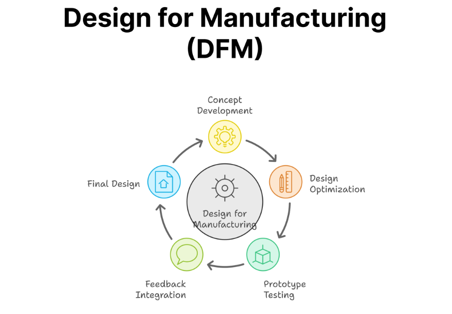
What is DFM and Why It Matters for PCBA Reliability
Design for Manufacturability (DFM) is an engineering approach focused on optimizing a product's design to make it easier, more efficient, and more cost-effective to produce. For Printed Circuit Board Assemblies, PCBA DFM guidelines encompass a wide range of considerations, from component selection and placement to PCB layout and process tolerances. The ultimate goal is to minimize manufacturing defects, reduce assembly time, and prevent issues that could compromise the PCBA's performance and lifespan.
The direct link between DFM and PCBA reliability is undeniable. A design that overlooks manufacturability often introduces hidden weaknesses that may not manifest immediately but can lead to failures over time or under specific operating conditions. For example, inadequate pad sizes can result in weak solder joints, while incorrect trace clearances can lead to shorts or opens. These subtle issues, when not addressed by thoughtful PCBA design optimization, directly degrade the PCBA's reliability. By embedding DFM principles early in the design phase, engineers proactively mitigate these risks, ensuring that each manufactured PCBA adheres to stringent quality standards and performs reliably throughout its intended operational life. This proactive approach to PCBA manufacturability is an investment in future product success.
Technical Principles: How DFM Prevents Defects and Enhances Reliability
The principles of DFM directly influence manufacturing quality by preventing common defects and inherently enhancing PCBA reliability. These technical considerations ensure that the design respects the physical realities and limitations of the assembly process.
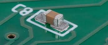
- Optimizing Component Spacing and Placement: Proper spacing between components, as defined by PCBA DFM guidelines, prevents solder bridging during reflow soldering, especially for fine pitch devices. It also ensures adequate clearance for automated pick and place nozzles and allows for visual inspection and rework. Components placed too close together can create thermal shadowing, leading to inconsistent solder joints, a significant cause of reliability issues.
- Robust Pad and Aperture Design: The design of component land patterns (pads) and the corresponding solder paste stencil apertures are critical. Properly sized pads facilitate optimal solder joint formation, while correctly designed stencil apertures ensure the right amount of solder paste is deposited. Deviations can lead to insufficient solder, voids, or excessive solder, all of which compromise joint strength and PCBA reliability. IPC-7351B, "Generic Requirements for Surface Mount Design and Land Pattern Standard," provides detailed specifications for land pattern design.
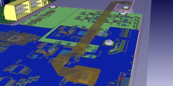
- Trace Routing and Clearance: Adhering to minimum trace widths and clearances prevents electrical shorts and opens. Incorrect routing can lead to impedance mismatches for high-speed signals, affecting performance and reliability. DFM also considers signal integrity, ensuring clean signal paths crucial for stable operation. IPC-2221B, "Generic Standard on Printed Board Design," offers guidance on these aspects.
- Panelization for Assembly: For smaller boards, panelization (arranging multiple PCBs on a larger panel) is a DFM technique that optimizes throughput. A well-designed panel minimizes stress on individual boards during de-panelization and handling, preventing micro-cracks or component damage that could impact long-term reliability.
- Thermal Management Integration: DFM for PCBA reliability includes proactive thermal management in the PCB layout. This involves strategic component placement, using thermal vias to dissipate heat, and designing proper copper planes as heat sinks. Preventing localized hot spots ensures components operate within their specified temperature ranges, extending their lifespan.
By rigorously applying these technical principles, DFM ensures that the PCBA manufacturability is maximized, directly translating into fewer defects and a higher standard of reliability.
Related Reading: Design for Manufacturability (DFM): The Key to Reducing PCB Component Assembly Costs
Practical Solutions and Best Practices for PCBA Design Optimization
Implementing effective PCBA DFM guidelines requires a systematic approach and collaboration across design and manufacturing teams. These practical solutions and best practices are key to successful PCBA design optimization.
- Early Collaboration: Engage manufacturing and assembly engineers early in the design cycle. Their practical insights into process capabilities, common failure modes, and assembly equipment limitations are invaluable for proactive DFM. This collaborative approach significantly contributes to PCBA design for reliability.
- Utilize DFM Software Tools: Leverage DFM analysis software to automatically check design rules, identify potential manufacturing violations, and generate reports. These tools can quickly pinpoint issues such as insufficient clearances, missing fiducials, or inadequate annular rings, which might be missed during manual review.
- Standardize Component Libraries: Develop and maintain a library of DFM-compliant component footprints and land patterns. Ensuring all designers use these optimized components reduces variability and guarantees proper solder joint formation, enhancing PCBA manufacturability.
- Follow Industry Standards: Adhere strictly to industry standards such as those published by IPC (Association Connecting Electronics Industries). IPC-A-610G, "Acceptability of Electronic Assemblies," provides visual criteria for acceptable soldered connections, while J-STD-001G, "Requirements for Soldered Electrical and Electronic Assemblies," outlines process requirements to achieve those standards. These documents are essential references for PCBA DFM guidelines.
- Prototyping and Feedback Loop: Even with DFM, prototypes are crucial. Use the prototype assembly process to gather feedback on manufacturability. Document any assembly challenges, rework requirements, or defects, and feed this information back into the design process for continuous PCBA design optimization.
- Surface Finish Selection: Choose the appropriate surface finish (e.g., ENIG, HASL, OSP) based on solderability requirements, shelf life, and cost. The surface finish directly impacts the quality of solder joints and protects the copper from oxidation, influencing long-term reliability.
By systematically applying these best practices, design teams can achieve significant improvements in PCBA manufacturability, leading to more robust and reliable products.
Related Reading: Avoiding Costly Mistakes: DFM Guidelines for Prototype PCB Assembly
The Broader Impact: Achieving PCBA Design for Reliability
DFM extends beyond merely avoiding immediate manufacturing defects; it is a critical component of achieving holistic PCBA design for reliability. A design optimized for manufacturability is inherently more robust and less prone to latent defects that could emerge under operational stress.
For instance, robust solder joint design, a key DFM output, directly impacts the PCBA's resilience to thermal cycling and mechanical vibration—common causes of failure in the field. When solder joints are consistently well-formed, with proper wetting and sufficient volume, they can withstand these stresses much more effectively. Conversely, poorly formed joints, often a result of DFM oversights, act as weak points, leading to premature fatigue and failure.
Moreover, DFM considerations for component placement and trace routing directly influence signal integrity and power delivery. A PCBA designed with DFM principles minimizes electrical noise, crosstalk, and voltage drops, ensuring stable and consistent performance across various operating conditions. This stability is a cornerstone of long-term reliability. The focus on PCBA manufacturability during the design phase thus reduces the likelihood of both manufacturing-induced defects and operational failures, ensuring the product maintains its integrity throughout its intended lifespan. This strategic approach minimizes warranty claims, enhances brand reputation, and ultimately contributes to customer satisfaction.
Conclusion
The pursuit of manufacturing excellence in Printed Circuit Board Assemblies is inextricably linked to the proactive implementation of Design for Manufacturability (DFM). By adhering to comprehensive PCBA DFM guidelines, engineers can systematically prevent defects, optimize assembly processes, and fundamentally enhance PCBA reliability. Through meticulous attention to component spacing, pad design, trace routing, and thermal management, DFM ensures that every PCBA is built to robust standards. This strategic PCBA design optimization approach is not merely about streamlining production; it is about embedding quality and dependability into the core of the product, minimizing costly failures, and guaranteeing long-term operational success for electronic devices.
FAQs
Q1: What are PCBA DFM guidelines?
A1: PCBA DFM guidelines are a set of rules and best practices used during the PCB design phase to optimize the board for efficient, cost-effective, and high-yield manufacturing and assembly. These guidelines cover aspects like component selection, placement, pad design, and trace routing to prevent manufacturing defects and enhance PCBA reliability.
Q2: How does DFM contribute to PCBA reliability?
A2: DFM significantly contributes to PCBA reliability by preventing common manufacturing defects such as solder shorts, opens, and weak solder joints, which are major causes of product failure. By optimizing the design for PCBA manufacturability, DFM ensures consistent quality in every assembled board, leading to more robust and dependable electronic products over their lifespan.
Q3: What is PCBA design optimization?
A3: PCBA design optimization involves refining the PCB layout, component choices, and material specifications to improve manufacturing efficiency, reduce costs, and enhance the overall performance and reliability of the assembled board. This process integrates PCBA DFM guidelines and other engineering principles to achieve the best possible outcome for the PCBA.
Q4: Why is early collaboration important for PCBA manufacturability?
A4: Early collaboration between design and manufacturing teams is crucial for PCBA manufacturability because it allows designers to incorporate practical production insights from the outset. This prevents potential manufacturing issues from being designed into the board, leading to fewer rework cycles, reduced costs, and a smoother transition from design to high-volume PCBA production.
References
IPC-A-610G — Acceptability of Electronic Assemblies. IPC, 2017.
IPC-2221B — Generic Standard on Printed Board Design. IPC, 2012.
IPC-7351B — Generic Requirements for Surface Mount Design and Land Pattern Standard. IPC, 2010.
J-STD-001G — Requirements for Soldered Electrical and Electronic Assemblies. IPC/JEDEC, 2017.
ISO 9001:2015 — Quality Management Systems. ISO, 2015.


