Introduction
In surface mount technology assembly, the PCB stencil plays a pivotal role in applying solder paste precisely onto pads. A poorly designed stencil can lead to defects such as solder bridging, insufficient paste volume, or tombstoning, which increase rework costs and delay production timelines. Engineers often overlook subtle design flaws that manifest during high-volume manufacturing. This article provides a comprehensive PCB stencil design checklist to help electric engineers identify and avoid common stencil design errors. By following a structured stencil design review process, teams can enhance yield rates and reliability. Mastering these stencil design best practices ensures seamless transition from design to assembly.
What Is PCB Stencil Design and Why It Matters
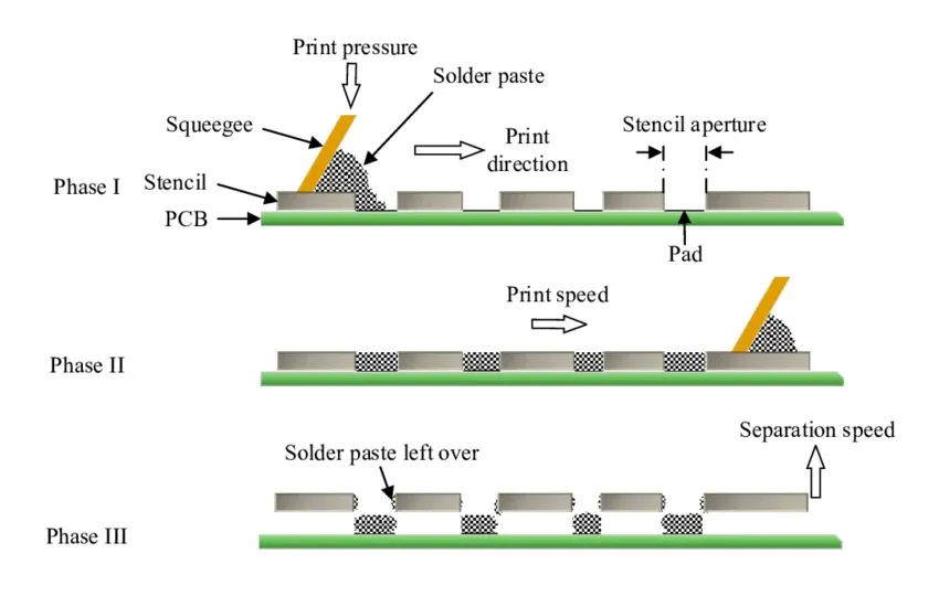
PCB stencil design involves creating a thin metal sheet, typically stainless steel, with precisely cut apertures that align with the board's solder pads. During printing, solder paste is squeegeed across the stencil, depositing paste only through the openings onto the PCB. This process directly influences the quality of solder joints formed in reflow soldering. Inaccurate stencil design disrupts paste transfer efficiency, leading to assembly failures that are expensive to rectify post-production. For electric engineers working on dense boards with fine-pitch components, optimal stencil design is crucial for achieving consistent volume control and minimizing defects. Adhering to industry guidelines like IPC-7525 ensures compatibility with automated assembly lines.
The relevance extends beyond initial prototyping to high-reliability applications in automotive and aerospace sectors. Faulty stencils contribute to up to significant portions of assembly rejects, amplifying costs through scrap and downtime. A robust design mitigates risks associated with varying paste rheologies and board warpage. Engineers must prioritize stencil parameters early in the PCB layout phase to avoid iterative revisions.
Key Technical Principles in PCB Stencil Design
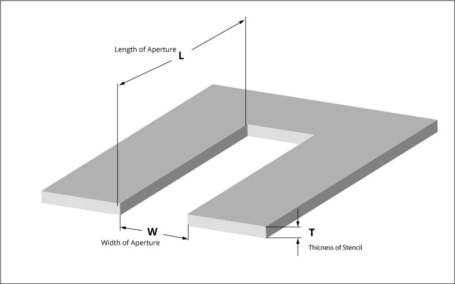
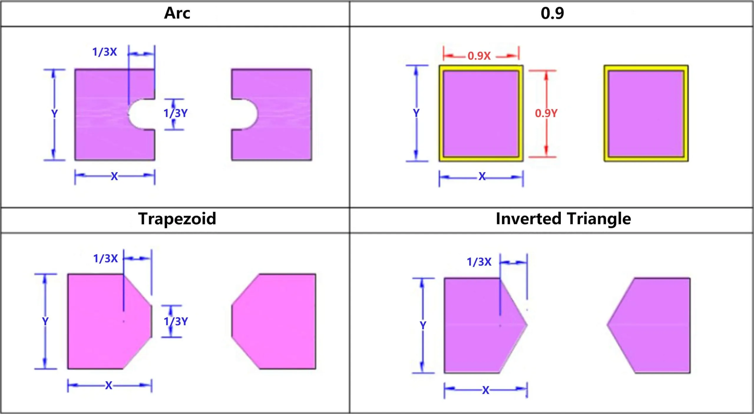
Stencil design hinges on balancing aperture geometry with printing dynamics to achieve uniform paste deposition. Aperture walls must promote clean release of solder paste, influenced by the powder-to-wall area ratio. Trapezoidal etching, where the bottom opening is narrower than the top, facilitates easier paste release during lift-off. Material selection favors nickel-coated stainless steel for durability and smoothness, resisting wear from repeated printing cycles. Frame rigidity prevents deformation under squeegee pressure, maintaining alignment accuracy.
Component-specific adaptations are essential, such as rounded corners or U-shapes for QFN and BGA packages to prevent paste smearing. Fiducial marks on the stencil match those on the PCB for precise registration during printing. Border widths around the frame accommodate machine clamps, while home positions aid stencil loading. Understanding these mechanisms allows engineers to predict behavior under varying gasketing forces and snap-off distances.
Common Stencil Design Errors and Their Causes
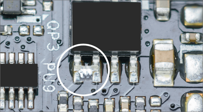
One prevalent error is matching stencil apertures exactly to pad sizes, which often results in excess paste leading to bridging on fine-pitch devices. Without reduction, paste bridges form between adjacent pads during reflow due to surface tension. Conversely, overly reduced apertures cause starvation, yielding weak joints prone to opens. Engineers frequently neglect pitch-dependent thickness choices, using uniform thicknesses across mixed-technology boards.
Another mistake involves ignoring via-in-pad configurations, where paste over tented vias contaminates the assembly process. Fiducials placed under components or omitted entirely disrupt alignment, causing offsets in paste printing. Inadequate border framing leads to stencil flexing, exacerbating warpage mismatches between stencil and PCB. Poor etching orientation can create burrs, trapping paste and causing inconsistent deposits. These common stencil design errors stem from insufficient review against manufacturing constraints.
Implementing a Stencil Design Review Process
A systematic stencil design review process begins with importing Gerber and drill files into analysis software to verify layer alignment. Check aperture fidelity against the solder mask and copper layers, ensuring no overlaps or omissions. Simulate paste volume calculations for critical components like BGAs, confirming compliance with volume targets. Evaluate area ratios and wall thicknesses to predict release performance.
Collaborate with assembly teams to validate fiducial placement and frame dimensions against printer specifications. Run design rule checks for minimum feature sizes and etching feasibility. Iterate based on feedback, documenting changes for traceability. This process uncovers latent issues before fabrication, saving costs. Final sign-off includes a dry-run alignment test if possible.
Stencil Design Best Practices and Software Considerations
Adopt these PCB stencil design best practices to optimize outcomes. Select stencil thickness inversely proportional to component pitch, thinner for finer pitches to control volume. Reduce aperture dimensions slightly relative to pads, typically five to twenty percent, adjusting per package type per IPC-7525 guidelines. Employ home plating on apertures to minimize solder balls by smoothing walls.
Incorporate sufficient fiducials, at least three, positioned away from edges and components. Define a robust frame with adequate borders for handling, and specify laser-cut over chemical etch for precision. Orient apertures to favor trapezoidal profiles during etching.
When evaluating stencil design software options, prioritize tools with automated aperture generation from Gerbers, built-in DFM rule sets, and paste volume calculators. Compare capabilities in handling complex geometries like QFNs, simulation of print defects, and export formats for fabricators. Features enabling rule-based reductions and batch processing streamline workflows for high-density boards. User interfaces supporting 3D visualization aid in spotting misalignment risks. Opt for software integrating land pattern standards like IPC-7351 for consistent pad-to-aperture mapping.
The Ultimate PCB Stencil Design Checklist
Use this comprehensive PCB stencil design checklist during reviews:
- Layer Verification: Confirm paste layer aligns perfectly with solder pads; exclude non-soldered areas like fiducials and vias.
- Aperture Geometry: Apply reductions, shapes, and orientations per component datasheets and pitch.
- Thickness Selection: Match to finest pitch; validate for mixed fine/coarse components.
- Fiducials and Registration: Ensure at least three marks, symmetric, with clear apertures.
- Frame and Borders: Minimum widths for clamps; rigid construction to resist deformation.
- Volume Control: Simulate brick heights and lengths for target joint profiles.
- Special Features: Home plating, bridges for multi-row QFNs, no paste over test points.
- DFM Compliance: Run checks for etchability, area ratios, and printer compatibility.
- Documentation: Include notes on material, thickness, and revisions.
Regularly audit against this list to preempt common stencil design errors.
Troubleshooting Common Assembly Issues from Stencil Flaws
Insufficient paste often traces to excessive aperture reductions or overly thin stencils, remedied by incremental enlargements and volume recalculations. Bridging signals thick stencils or square apertures; switch to trapezoidal and verify squeegee speed. Tombstoning arises from uneven paste heights across components, addressed by balanced reductions.
For QFN voids, implement U-shaped or scooped apertures to enhance paste flow under the package. If offsets occur, reposition fiducials or enlarge their stencil openings. Board warpage mismatches require frame adjustments or thinner stencils. Systematic troubleshooting links defects back to design, enabling targeted fixes.
Conclusion
Effective PCB stencil design demands attention to apertures, thickness, and registration to avoid costly assembly pitfalls. By integrating the provided checklist and review process into workflows, electric engineers can achieve higher first-pass yields. Leverage stencil design best practices aligned with IPC standards for reliability. Even generic software comparisons highlight the value of automation in rule enforcement. Prioritizing these elements transforms stencil design from a potential bottleneck into a strength, supporting efficient production scaling.
FAQs
Q1: What is the most critical step in the PCB stencil design checklist?
A1: Verifying aperture geometry against pad sizes tops the list, as mismatches cause bridging or starvation. Cross-check reductions for fine-pitch parts using simulation tools. This prevents common stencil design errors early. Follow with fiducial alignment to ensure printing accuracy.
Q2: How does the stencil design review process identify common stencil design errors?
A2: Import Gerbers and run DFM checks for overlaps, ratios, and volumes. Simulate prints to spot bridging risks. Consult assembly input on printer limits. Iterate until compliant with guidelines like IPC-7525. This proactive approach minimizes defects.
Q3: What features matter in a stencil design software comparison?
A3: Look for auto-reduction rules, 3D paste visualization, and IPC-compliant libraries. Batch processing for panels saves time. Integration with land patterns from IPC-7351 ensures consistency. Defect prediction modules aid troubleshooting. Prioritize ease for complex boards.
Q4: Why follow stencil design best practices for fine-pitch components?
A4: Fine-pitch demands thinner stencils and precise reductions to control paste volume. Trapezoidal apertures improve release. Neglect leads to rework-heavy bridging. Best practices per industry standards boost yield on dense assemblies.
References
IPC-7525C — Stencil Design Guidelines. IPC, 2021
IPC-7351C — Generic Requirements for Surface Mount Design and Land Pattern Standard. IPC, 2010
IPC-A-610H — Acceptability of Electronic Assemblies. IPC, 2019