Introduction
Leaded solder alloys remain a cornerstone in certain PCB assembly processes, particularly where lead-free alternatives fall short in reliability or process control. These alloys, primarily tin-lead combinations, offer predictable melting behavior and robust joint integrity that electric engineers value in high-stakes applications like aerospace and military electronics. Despite regulatory shifts toward lead-free soldering, leaded options persist in exempted sectors due to their proven performance under thermal cycling and vibration. This guide breaks down leaded solder alloy charts, compositions, and selection criteria to help you optimize wave and reflow soldering outcomes. Understanding these factors ensures fewer defects like cold joints or bridging during assembly.
What Are Leaded Solder Alloys and Why Do They Matter in PCB Assembly?
Leaded solder alloys consist mainly of tin (Sn) and lead (Pb), often with minor additions like silver (Ag) for enhanced properties. They form the basis for reliable electrical and mechanical connections on printed circuit boards by wetting pads and component leads effectively. In PCB assembly, these alloys excel because their eutectic formulations melt at a single temperature, minimizing risks of incomplete melting or residue. Electric engineers prefer them for troubleshooting scenarios where joint fillet formation must be consistent across mixed-technology boards. Their ductility also absorbs stresses from thermal expansion mismatches between components and substrates. As regulations evolve, selecting the right mix aligns with performance needs while adhering to exemptions in critical industries.
The relevance stems from superior wettability and lower processing temperatures compared to some lead-free counterparts, reducing board warpage and component damage. In wave soldering lines, leaded solders flow smoothly over through-hole leads, forming shiny, concave fillets indicative of good adhesion. For reflow, they support precise peak temperature control, avoiding overheating sensitive parts. Engineers troubleshooting failures often trace issues back to alloy mismatch, such as using a non-eutectic blend that solidifies prematurely. Practical testing confirms that leaded alloys maintain conductivity and strength over extended lifecycles in vibrating environments.
Leaded Solder Composition Guide: Key Alloys for PCB Use
A leaded solder composition guide starts with the most common binary SnPb alloys, classified under industry standards for electronic-grade purity. Sn63Pb37 represents the eutectic point, with 63% tin and 37% lead, ideal for sharp melting transitions. Sn60Pb40 shifts to 60% tin and 40% lead, offering a slight plastic range for self-leveling in selective soldering. Ternary SnPbAg variants, like Sn62Pb36Ag2, incorporate 2% silver to boost fatigue resistance without altering flow much. These compositions ensure low oxide formation and compatibility with common fluxes in assembly lines.
Here's a leaded solder alloy chart summarizing prevalent options:
- Sn63Pb37 — Composition: 63Sn-37Pb; Common Forms: Bar, Wire, Paste; Typical Applications: Wave, Reflow, Hand Soldering
- Sn60Pb40 — Composition: 60Sn-40Pb; Common Forms: Bar, Wire, Paste; Typical Applications: Wave, Selective Soldering
- Sn62Pb36Ag2 — Composition: 62Sn-36Pb-2Ag; Common Forms: Bar, Wire, Paste; Typical Applications: High-Reliability Reflow
- Sn50Pb50 — Composition: 50Sn-50Pb; Common Forms: Paste, Preforms; Typical Applications: High-Temperature Joints
Deviations from these ratios affect viscosity and joint voids, so verify supplier specs against assembly requirements. In practice, start with Sn63Pb37 for prototypes to baseline performance before scaling.
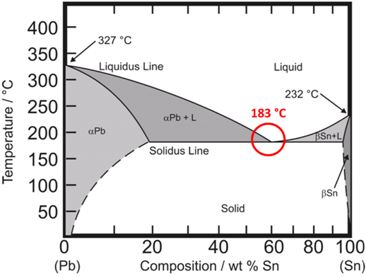
Leaded Solder Melting Temperatures: Eutectic vs. Non-Eutectic Behavior
Leaded solder melting temperatures center around 183°C for eutectic blends, enabling reflow profiles below 220°C peak to protect components. Sn63Pb37 melts precisely at 183°C solidus and liquidus, transitioning instantly from solid to fully liquid for optimal fillet formation. Non-eutectic Sn60Pb40 exhibits a range of 183°C to 191°C, staying semi-liquid longer to bridge gaps but risking skulling on wave pots. Sn62Pb36Ag2 lowers this slightly to 179-181°C, aiding heat-sensitive assemblies. These temperatures dictate preheat zones and conveyor speeds in production.
Engineers troubleshoot overheating by plotting thermal profiles; eutectics forgive minor oven variances better than wide-range alloys. Always factor in flux activation, as residues shift effective melting by 5-10°C.
Mechanical Properties: Focus on Leaded Solder Tensile Strength
Leaded solder tensile strength varies by composition, with SnPbAg outperforming binaries in creep resistance for vibrating PCBs. Sn63Pb37 delivers around 8720 psi ultimate tensile strength and 6200 psi shear, balancing ductility at 37% elongation. Sn60Pb40 offers 7280 psi tensile and 5600 psi shear, with 24% elongation suiting flexible joints. The Sn62Pb36Ag2 alloy excels at 10910 psi tensile and 7540 psi shear, plus 114% elongation for fatigue-prone apps. These values, measured per standardized tests, predict joint reliability under load.
In troubleshooting, low tensile often signals contamination; test lap shear on scrap boards to qualify lots. Silver additions enhance grain refinement, reducing voids that weaken strength over cycles.
Best Leaded Solder for Wave Soldering: Process Optimization
The best leaded solder for wave soldering is Sn63Pb37 bar solder, prized for its eutectic nature and low dross generation in pots held at 245-260°C. Its instant liquidity ensures clean hole fill and minimal icicles on through-hole components. Sn60Pb40 serves as an alternative where bridging needs correction via plastic flow before full solidification. Preheat boards to 100-120°C to match alloy temps, avoiding thermal shock. Flux compatibility is key; no-clean types pair well without post-clean residue buildup.
Troubleshoot wave defects by alloy purity; impurities raise melting, causing dewetting. Monitor pot chemistry weekly for consistent drag-out.
Leaded Solder for Reflow Soldering: Profile and Paste Selection
Leaded solder for reflow soldering favors Sn63Pb37 paste, with reflow peaks at 210-225°C and 60-90 second above liquidus. This alloy's flow wets fine-pitch QFPs without tombstoning, common in mixed assemblies. Sn62Pb36Ag2 paste adds strength for BGA underfill alternatives. Ramp rates of 1-2°C/s prevent flux splatter. Vapor phase works well for uniform heating on dense boards.
Profile voids by thermocouple mapping; adjust soak for stencil release. Post-reflow X-ray checks solder volume against IPC criteria.
SnPbAg Solder Alloys: Enhanced Performance Options
SnPbAg solder alloys like Sn62Pb36Ag2 improve tensile strength and thermal fatigue resistance over pure binaries. The 2% silver refines microstructure, suppressing lead-rich phases that creep under load. Melting at 179°C suits hybrid leaded/lead-free lines. Use in high-vibration modules where elongation prevents cracking. Cost-benefit favors them for long-life products.
Select based on J-STD-006C classifications for impurity limits.
Standards Compliance and Best Practices
Adhere to J-STD-006C for electronic-grade leaded solder alloys, ensuring disclosed compositions and low impurities. IPC-A-610 guidelines define acceptable joint appearances, like 100% heel fillet in wave. Qualify alloys via wetting balance tests before production. Store bars in dry conditions to prevent oxidation. For mixed assemblies, segregate leaded zones with pallets.
Practical tip: Simulate profiles on demo boards to catch alloy-process mismatches early. Document deviations for traceability.
Conclusion
Choosing the right leaded solder alloy hinges on process type, with Sn63Pb37 as a versatile default for wave and reflow. Consult leaded solder alloy charts for melting and strength matches to your PCB demands. SnPbAg options elevate reliability in demanding environments. Follow standards for consistent results, minimizing rework. This approach yields durable assemblies that electric engineers can trust.
FAQs
Q1: What does a leaded solder alloy chart reveal for PCB selection?
A1: A leaded solder alloy chart displays compositions like Sn63Pb37 alongside melting points and forms, guiding wave or reflow choices. It highlights eutectic alloys for sharp transitions versus plastic-range for bridging fixes. Use it to match tensile strength to vibration needs, ensuring J-STD-006C compliance. Always cross-check with your flux and profile.
Q2: How does the leaded solder composition guide influence wave soldering?
A2: The leaded solder composition guide recommends Sn63Pb37 for optimal flow and low dross in wave pots. Higher lead like Sn60Pb40 aids self-healing of bridges. Balance tin content for wetting without skulling. Preheat aligns with solidus for defect-free holes. Troubleshoot via fillet inspection per IPC-A-610.
Q3: What is the best leaded solder for wave soldering and why?
A3: Sn63Pb37 stands as the best leaded solder for wave soldering due to its 183°C eutectic melt and superior fluidity. It forms reliable through-hole joints with minimal icicles. Compared to Sn60Pb40, it reduces variability in high-volume runs. Pot temps at 250°C maximize performance.
Q4: Why consider leaded solder tensile strength in SnPbAg alloys?
A4: Leaded solder tensile strength in SnPbAg alloys like Sn62Pb36Ag2 reaches higher values with better elongation, resisting fatigue in PCBs. Silver refines grains for creep resistance. Evaluate via shear tests for your loads. It outperforms binaries in thermal cycling, per standard quals.
References
J-STD-006C — Requirements for Electronic Grade Solder Alloys and Fluxed and Non-Fluxed Solders. IPC/JEDEC
IPC-A-610G — Acceptability of Electronic Assemblies. IPC


