Introduction
In surface mount technology assembly, stencil apertures play a pivotal role in achieving precise solder paste deposition. Engineers often grapple with optimizing these apertures to ensure consistent solder paste release, which directly impacts first-pass yields and defect rates. This guide delves into the critical distinction between stencil aspect ratio and stencil area ratio, two fundamental parameters that dictate paste transfer efficiency. Understanding their differences and applications helps troubleshoot common printing issues in high-density boards. We will explore definitions, calculations, aperture design guidelines, and practical strategies tailored for electric engineers working with SMT stencils. By mastering these ratios, you can enhance assembly reliability and reduce rework.
What Are Stencil Aspect Ratio and Area Ratio?
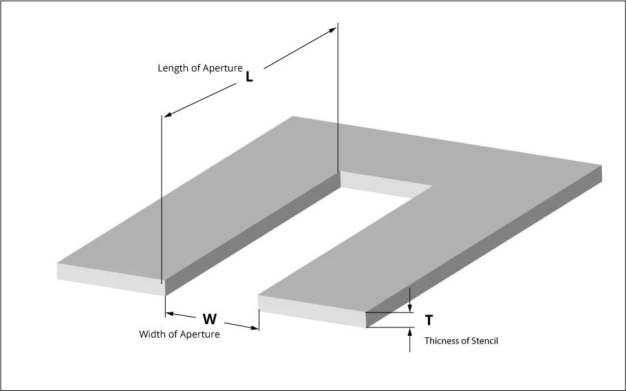
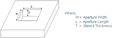
Stencil aspect ratio refers to the ratio of the smallest dimension of the aperture opening to the stencil thickness. For rectangular apertures, this is typically the width divided by thickness, with industry guidelines recommending a minimum value greater than 1.5 for reliable performance. In contrast, stencil area ratio provides a more comprehensive metric by comparing the open area of the aperture to the total surface area of the aperture walls. This ratio accounts for the entire perimeter and is calculated as the aperture area divided by the product of the perimeter and stencil thickness. Both ratios serve as predictors of solder paste release, but area ratio offers better accuracy for irregular shapes. Electric engineers use these to evaluate aperture viability before fabrication. Aspect ratio simplifies initial checks, especially for elongated apertures common in fine-pitch components. However, it overlooks perimeter effects, making it less precise for complex geometries. Area ratio, while more involved, captures the full interaction between paste and stencil walls during printing. IPC-7525B outlines these definitions clearly, emphasizing their role in stencil design guidelines. Mastering both ensures apertures support high-volume production without compromising quality.
Why Stencil Ratios Matter for Solder Paste Release
Solder paste release efficiency hinges on the balance between aperture volume and wall adhesion forces. When ratios fall below recommended thresholds, paste clings to stencil walls, resulting in insufficient deposits, bridging, or voids after reflow. High aspect or area ratios promote clean snap-off, where over 75 percent transfer is typical for type 3 or 4 pastes, though exact efficiencies vary with rheology. In fine-pitch SMT, poor ratios amplify defects like tombstoning or head-in-pillow, escalating scrap rates. Engineers prioritize these metrics during design reviews to preempt assembly failures. Ultimately, optimized ratios align with process windows for consistent joint formation.
Low ratios exacerbate issues with high-metal-content pastes used in lead-free processes. Wall friction and cohesive forces dominate in narrow, deep apertures, trapping particles. Conversely, favorable ratios leverage paste's thixotropy for smooth release. Troubleshooting starts here: measure ratios first when prints show inconsistencies. This approach saves time over iterative printing trials.
Technical Principles: Calculating Aspect and Area Ratios
To calculate stencil aspect ratio, divide the aperture's minimum width by stencil thickness. For a 0.4 mm wide aperture in a 0.1 mm thick stencil, the ratio is 4, well above the 1.5 threshold. Rectangular apertures use the smaller of length or width. Circular apertures treat diameter as the width. This metric flags overly narrow features early.
Area ratio demands aperture area over wall area: for rectangles, (length times width) divided by [2 times (length plus width) times thickness]. A 0.5 mm by 0.5 mm square in 0.1 mm thickness yields (0.25) / [2 * (1) * 0.1] = 1.25, exceeding 0.66. Circles simplify to radius over twice thickness. IPC-7525B recommends area ratio greater than 0.66 for most applications. Software tools automate these, but manual verification ensures accuracy.
These formulas assume uniform wall finish and standard laser-cut stencils. Variations in electroformed or nano-coated walls may adjust effective ratios slightly. Engineers compute for all apertures, prioritizing smallest ones. Batch analysis reveals design flaws before procurement.
Aperture Design Guidelines for SMT Stencils
Adhere to aspect ratio above 1.5 by selecting thinner stencils for fine-pitch leads below 0.5 mm. Standard thicknesses range from 0.1 to 0.15 mm, balancing volume and release. For area ratio, elongate narrow apertures or truncate corners to boost open area relative to perimeter. IPC-7525B provides these stencil aperture design guidelines, stressing geometry tweaks. [2] (https://webstore.ansi.org/preview-pages/IPC/preview_IPC+7525B-2011.pdf?srsltid=AfmBOopuzZruMu-TdqWfLvCmLQkG8QDWJ1IA4Um_ZsfZvUI1J7I2p3sv)
Home-plate shapes suit QFN peripherals, increasing ratio by 10-20 percent over rectangles without altering pad footprint. U-shaped or scooped designs aid central pads in large BGAs. Maintain minimum land-aperture offsets per land pattern standards. Test ratios across component libraries.
- Rectangular: Aspect ratio guideline > 1.5 (width / T); Area ratio guideline > 0.66; common use: QFP, SOIC.
- Square: Aspect ratio guideline > 1.5 (side / T); Area ratio guideline > 0.66; common use: CSP.
- Circular: Aspect ratio guideline > 1.5 (diameter / T); Area ratio guideline > 0.66; common use: vias.
- Oblong: Aspect ratio guideline > 1.5 (minimum dimension / T); Area ratio guideline > 0.66; common use: QFN edges.
This list summarizes quick checks. Deviations require validation prints.
Best Practices and Troubleshooting for Optimal Ratios
Start with stencil thickness selection: 0.1 mm for pitches under 0.4 mm to preserve ratios. Verify all apertures exceed thresholds using spreadsheets. Incorporate step-stencils for mixed technologies, thinning fine-pitch zones. Clean stencils every 5-10 prints to sustain release.
If bridging occurs, inspect area ratios on adjacent apertures; low values promote bridging. Insufficient paste volume signals aspect ratio shortfalls, prompting redesign. Poor release in corners? Round them to cut perimeter. Process tweaks like slower snap-off help marginal ratios temporarily.
Profile paste rheology against stencil specs. Collaborate with fabricators on wall quality. Document ratios in design files for traceability.
Common Troubleshooting Scenarios
Consider a fine-pitch BGA with 0.3 mm apertures in 0.125 mm stencil: aspect ratio drops below 2.4, risking voids. Solution: thin to 0.1 mm, recalculating area ratio to 0.75. Another case: elongated QFN pads yield low area ratio due to high perimeter. Adopt home-plate, lifting ratio to compliant levels.
Persistent sticking? Audit wall finish; rough surfaces tank effective ratios. Overprinting? Ratios fine, but speed or pressure culprit. Systematic checks isolate root causes efficiently.
Post-reflow inspection correlates back to ratios. Iterate designs proactively.
Conclusion
Stencil aspect ratio and area ratio form the cornerstone of effective SMT stencil design, directly governing solder paste release. Aspect ratio offers a quick geometric check, while area ratio delivers precise prediction across shapes. Following guidelines like those in IPC-7525B ensures high yields in demanding assemblies. Engineers should integrate ratio calculations into workflows, pairing with practical tweaks for challenging features. This disciplined approach minimizes defects and streamlines production. Apply these insights to elevate your PCB assembly outcomes.
FAQs
Q1: What is the difference between stencil aspect ratio and stencil area ratio?
A1: Stencil aspect ratio is the minimum aperture width divided by stencil thickness, targeting above 1.5 for basic feasibility. Stencil area ratio expands this to aperture area over wall surface area, requiring over 0.66 for optimal solder paste release. Aspect suits quick screens; area handles complex perimeters better. Use both in aperture design guidelines to predict printing success.
Q2: How do you calculate area ratio for SMT stencil apertures?
A2: For rectangles, divide length times width by 2 times (length plus width) times thickness. Circles use πr2 over 2πr times thickness, simplifying to r / (2T). Aim for greater than 0.66 per IPC standards to ensure clean release. Verify smallest apertures first in fine-pitch designs.
Q3: What are ideal stencil aspect ratio values for fine-pitch components?
A3: Target above 1.5, often 2 or higher for pitches under 0.4 mm by thinning stencils to 0.1 mm. This prevents paste trapping while maintaining volume. Combine with area ratio checks for comprehensive aperture design guidelines. Adjust shapes if ratios falter.
Q4: Why is solder paste release poor despite good stencil aspect ratio?
A4: Aspect ratio alone ignores perimeter; low area ratio traps paste on walls. Check full calculations, wall finish, and paste type. Troubleshoot with step-stencils or geometry modifications. IPC-7525B ratios guide resolutions effectively.
References
IPC-7525B — Stencil Design Guidelines. IPC, 2011.