Introduction
In the realm of multi-layer PCB design, achieving optimal performance requires meticulous attention to grounding and signal integrity. Via stitching stands as a critical technique for electrical engineers to enhance these aspects, particularly in high-speed design environments. This method involves placing multiple vias to connect ground planes across layers, effectively reducing electromagnetic interference (EMI) and ensuring stable signal paths. As modern electronics demand faster data rates and compact layouts, understanding via stitching becomes indispensable for minimizing noise and maintaining reliable operation. This comprehensive guide explores the principles of via stitching, its importance in grounding, and best practices for implementation. Aimed at electrical engineers, the article provides actionable insights to optimize multi-layer PCB designs for EMI reduction and robust performance in demanding applications.
What Is Via Stitching and Why It Matters
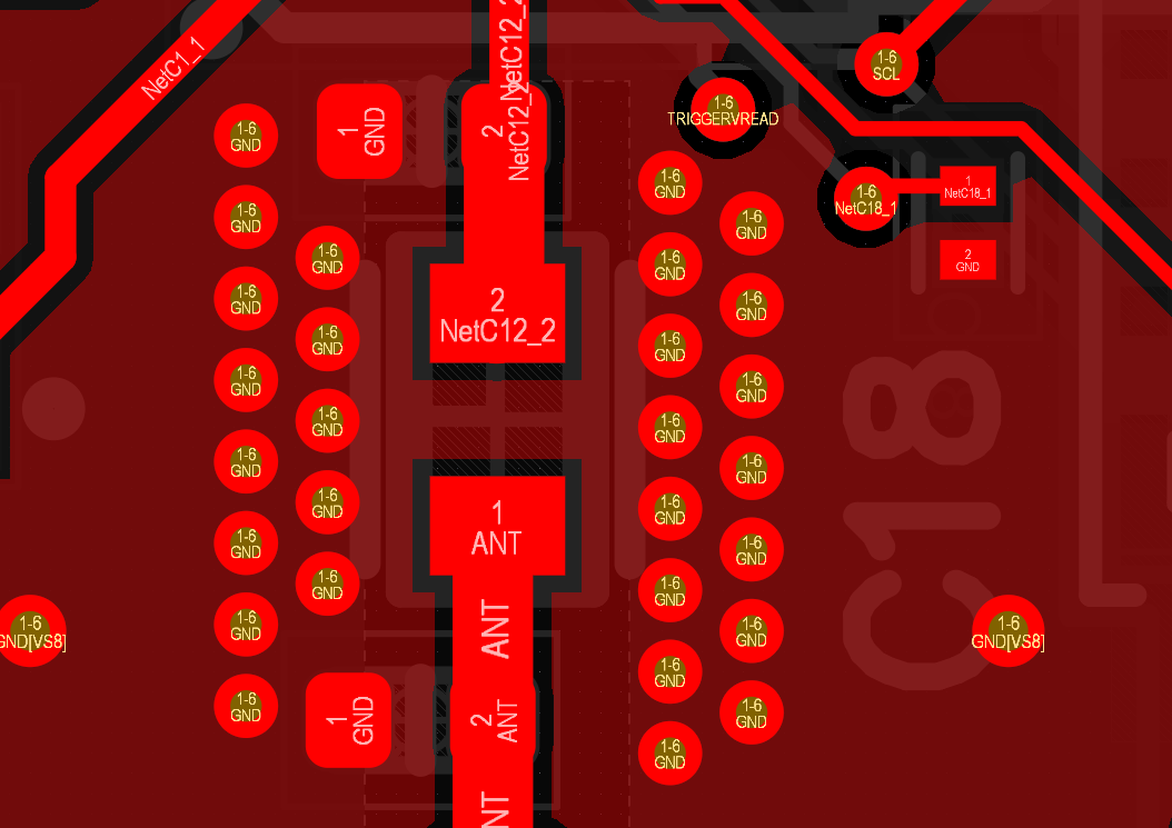
Via stitching refers to the strategic placement of multiple vias in a multi-layer PCB to connect ground planes or power planes across different layers. These vias act as low-impedance paths, ensuring continuity of reference planes and minimizing disruptions in signal return paths. In high-speed design, where signals switch at rapid rates, maintaining a consistent ground plane is vital to prevent noise coupling and signal distortion. Without proper grounding, high-frequency signals can generate EMI, leading to performance degradation or system failure.
The significance of via stitching lies in its ability to enhance signal integrity and achieve EMI reduction. By creating a robust network of ground connections, it reduces loop inductance and provides a direct path for return currents. This is especially crucial in multi-layer PCB layouts, where signals often transition between layers, risking impedance mismatches. For engineers working on complex designs, implementing via stitching is a fundamental step to ensure reliability and compliance with stringent performance standards.
Technical Principles of Via Stitching
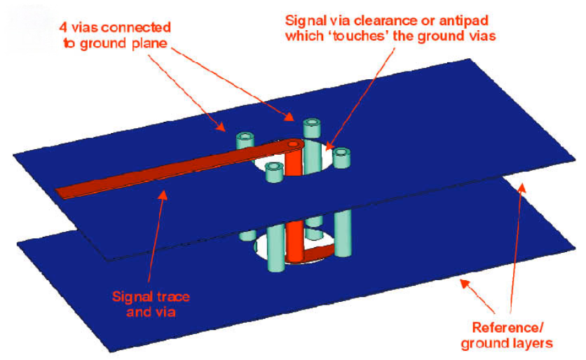
The core principle behind via stitching is to maintain a uniform reference plane for signals, particularly in high-speed design scenarios. When a signal trace transitions between layers through a via, the return current must follow a path through the nearest ground plane. If the ground plane is discontinuous or poorly connected, the return path becomes longer, increasing inductance and creating potential for noise. Via stitching addresses this by placing vias around signal vias or along the edges of ground planes, forming a grid-like connection that minimizes impedance.
In terms of EMI reduction, via stitching helps by creating a Faraday cage effect around sensitive areas of the PCB. This containment reduces the radiation of electromagnetic fields from high-speed signals. Additionally, it lowers the risk of crosstalk between adjacent traces by providing a stable ground reference. The spacing and density of stitched vias are critical factors, as they determine the effectiveness of grounding. Typically, closer spacing is preferred for higher frequencies to ensure low-impedance connections.
Another key aspect is thermal management. In multi-layer PCB designs handling high currents, via stitching can aid in heat dissipation by connecting to large copper areas. This dual role of electrical and thermal performance makes it a versatile technique. Engineers must consider the via size, drill diameter, and placement to balance manufacturing constraints with electrical requirements, adhering to recognized industry guidelines for optimal results.
Related Reading: Via Stitching: A Comprehensive Guide to Enhancing Grounding and Shielding in PCBs
Best Practices for Via Stitching in Multi-Layer PCBs
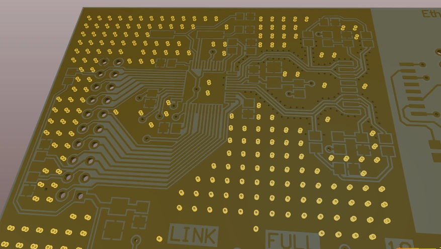
Optimize Via Placement and Spacing
Place stitched vias strategically around high-speed signal vias to provide a short return path for currents. A common practice is to arrange vias in a grid pattern near the edges of ground planes or along critical signal paths. For high-speed design, spacing between vias should be kept small, often a fraction of the wavelength of the highest signal frequency, to maintain low impedance. This prevents the formation of resonant structures that could amplify EMI.
Ensure Continuity of Ground Planes
In multi-layer PCB layouts, ensure that ground planes on adjacent layers are connected through stitched vias at regular intervals. This continuity is essential for maintaining a consistent reference for signals and preventing ground bounce. Avoid large gaps in ground planes, as they can disrupt return paths and degrade signal integrity. If a ground plane is split for functional reasons, use stitched vias to bridge the sections wherever possible.
Match Via Density to Frequency Requirements
The density of stitched vias should correspond to the operating frequency of the design. For low-frequency applications, fewer vias spaced farther apart may suffice. However, in high-speed design scenarios, denser via stitching is necessary to handle rapid signal transitions and minimize noise. As a general guideline, follow industry standards such as those outlined in IPC-2221B for via placement in high-frequency designs.
Consider Manufacturing Constraints
While dense via stitching enhances electrical performance, it can complicate manufacturing and increase costs. Balance the number of vias with fabrication capabilities, ensuring that drill sizes and aspect ratios comply with guidelines like those in IPC-6012E. Smaller vias may be preferred for high-density designs, but they must be manufacturable without risking reliability. Collaborate with fabrication teams to align design choices with production limits.
Use Stitching for Power Planes When Necessary
Although via stitching is primarily associated with grounding, it can also be applied to power planes in multi-layer PCB designs. Connecting power planes across layers with vias helps maintain stable voltage levels and reduces noise in power distribution networks. This is particularly useful in designs with high current demands, where voltage drops can impact performance. Ensure that power plane vias are isolated from ground vias to avoid short circuits.
Simulate and Validate Designs
Before finalizing a design, use simulation tools to analyze the effectiveness of via stitching on signal integrity and EMI reduction. Simulations can reveal potential issues such as resonant frequencies or inadequate grounding. Validate the placement and density of vias against performance metrics, adjusting as needed to meet design goals. This step is crucial for high-speed design, where small errors can lead to significant problems.
Adhere to Industry Standards
Follow established standards to ensure the reliability of via stitching implementations. For instance, IPC-A-600K provides criteria for acceptability of printed boards, including via structures. Similarly, IPC-2221B offers guidance on design considerations for multi-layer PCB layouts. Adhering to these standards ensures that designs meet quality benchmarks and perform reliably in real-world applications.
Related Reading: Mastering PCB Routing: A Comprehensive Guide to Via Stitching Techniques
Challenges and Troubleshooting in Via Stitching
Despite its benefits, via stitching can present challenges that engineers must address during the design phase. One common issue is over-stitching, where excessive vias lead to unnecessary manufacturing complexity without significant performance gains. To avoid this, evaluate the frequency and signal requirements before determining via density. Another challenge is via stub effects, where unterminated vias act as antennas, radiating noise. Mitigate this by using back-drilling techniques or optimizing layer transitions.
Signal integrity issues may arise if stitched vias are unevenly distributed, creating impedance mismatches. Regularly spaced vias and thorough simulation can prevent such problems. Additionally, ensure that vias do not interfere with critical components or traces, as poor placement can introduce parasitic capacitance. If EMI persists despite stitching, inspect the overall layout for other noise sources, such as long signal loops or inadequate decoupling.
Conclusion
Via stitching remains a cornerstone technique for electrical engineers working on multi-layer PCB designs. By enhancing grounding and ensuring signal integrity, it addresses critical challenges in high-speed design and achieves effective EMI reduction. Through strategic placement, appropriate density, and adherence to industry standards, engineers can optimize their layouts for performance and reliability. Understanding the principles and best practices of via stitching empowers designers to tackle complex projects with confidence. As electronic systems continue to evolve, mastering this technique will be essential for delivering robust and efficient solutions in demanding applications.
FAQs
Q1: What is the primary purpose of via stitching in multi-layer PCB designs?
A1: Via stitching in multi-layer PCB designs primarily serves to connect ground planes across layers, ensuring a low-impedance path for return currents. This enhances grounding, improves signal integrity, and aids in EMI reduction by minimizing noise and loop inductance. It is especially critical in high-speed applications where consistent reference planes are necessary for reliable performance.
Q2: How does via stitching impact signal integrity in high-speed design?
A2: Via stitching significantly improves signal integrity in high-speed design by providing a stable ground reference and reducing return path disruptions. It minimizes impedance mismatches during layer transitions and lowers noise coupling between traces. Properly implemented stitching ensures cleaner signal transmission, which is vital for maintaining performance in fast-switching circuits.
Q3: What are key considerations for via stitching to achieve EMI reduction?
A3: To achieve EMI reduction through via stitching, focus on placing vias close to high-speed signal paths and maintaining uniform spacing. A grid pattern near ground plane edges helps contain electromagnetic fields. Additionally, ensure continuity between layers to avoid radiation points. Following industry guidelines for via density based on frequency also enhances effectiveness.
Q4: How should via stitching be balanced with manufacturing constraints in multi-layer PCB layouts?
A4: Balancing via stitching with manufacturing constraints in multi-layer PCB layouts involves optimizing via count and size to avoid production issues. Consult fabrication guidelines, such as those in recognized standards, to ensure drill sizes and aspect ratios are feasible. Prioritize critical areas for stitching while minimizing unnecessary vias to keep costs and complexity manageable.
References
IPC-2221B — Generic Standard on Printed Board Design. IPC, 2012.
IPC-6012E — Qualification and Performance Specification for Rigid Printed Boards. IPC, 2020.
IPC-A-600K — Acceptability of Printed Boards. IPC, 2020.