Introduction
Step-up stencil printing plays a critical role in modern PCB assembly, particularly when dealing with mixed-component designs that require varying solder paste volumes. This specialized technique uses stencils with different thicknesses in specific areas to accommodate components with diverse height and pitch requirements. While effective, step-up stencils often encounter challenges like solder bridging, insufficient solder paste, paste smearing, misalignment, and cleaning difficulties. For electrical engineers, understanding and resolving these issues is essential to ensure high-quality surface mount technology (SMT) assembly and reliable board performance. This article dives into the technical aspects of step-up stencil printing, identifies common problems, and offers practical solutions to optimize the process. By addressing these concerns, engineers can achieve consistent results and minimize defects in PCB production.
What Is Step-Up Stencil Printing and Why It Matters
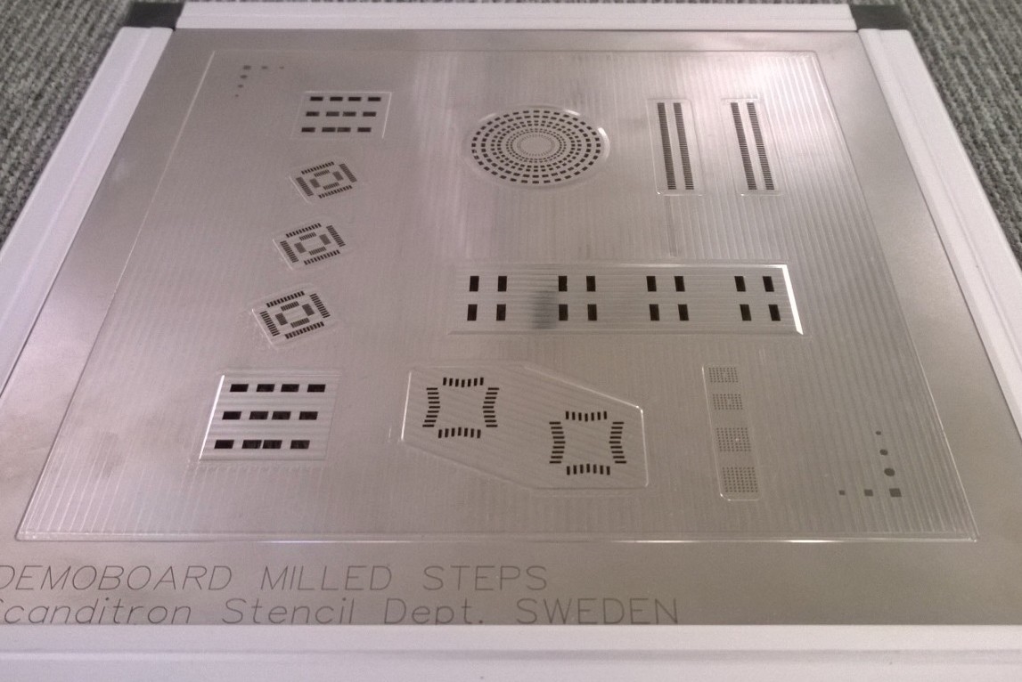
Step-up stencil printing is a variation of standard SMT stencil printing. Unlike uniform stencils, step-up stencils feature areas with increased thickness, often created through etching or additive processes, to deposit more solder paste for larger components like connectors or power devices. This approach ensures adequate solder volume for robust joints while maintaining precision for finer-pitch components. The technique is vital in mixed-technology boards where component diversity demands tailored paste application. Without proper execution, however, issues like step-up stencil solder bridging or insufficient solder can compromise assembly quality. For electrical engineers, mastering this process is key to meeting stringent reliability standards and ensuring functionality in complex electronic designs. The importance lies in balancing precision and volume to prevent defects that could lead to costly rework or failures.
Technical Principles Behind Step-Up Stencil Printing Issues
Understanding the root causes of problems in step-up stencil printing requires a grasp of the underlying mechanisms. The design of a step-up stencil introduces variations in thickness, typically ranging between standard and elevated zones. These variations affect solder paste release, pressure distribution during printing, and stencil durability. Below are the primary technical factors contributing to common issues.
Solder Paste Behavior and Volume Control
Solder paste transfer efficiency depends on the stencil aperture design and thickness. In step-up areas, thicker stencil zones aim to deposit more paste, but improper aperture ratios can cause uneven release. This often results in step-up stencil insufficient solder for larger pads or excessive paste leading to step-up stencil solder bridging between closely spaced pads.
Pressure and Squeegee Dynamics
During printing, the squeegee applies pressure to force solder paste through stencil apertures. In step-up stencils, uneven thickness can create inconsistent pressure distribution. Excessive force in thinner areas may cause step-up stencil paste smearing, while inadequate pressure in thicker zones can lead to incomplete paste transfer. This imbalance often exacerbates defects across the board.
Alignment and Registration Challenges
Precise alignment between the stencil and PCB is critical. Step-up designs, with their complex geometries, are prone to step-up stencil misalignment if the printing equipment lacks sufficient accuracy or if the stencil warps over time. Misalignment disrupts paste placement, causing defects like bridging or insufficient solder on critical pads.
Stencil Wear and Cleaning Complications
Step-up stencils endure significant mechanical stress due to repeated printing cycles. The varying thicknesses can lead to uneven wear, making step-up stencil cleaning more challenging. Residual paste in thicker areas or micro-cracks in transition zones can contaminate subsequent prints, leading to defects if not addressed through proper maintenance protocols.
Common Issues in Step-Up Stencil Printing
Electrical engineers frequently encounter specific defects when using step-up stencils. Identifying these problems and their symptoms is the first step toward effective troubleshooting.
Step-Up Stencil Solder Bridging
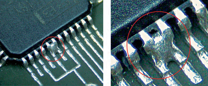
This defect occurs when excess solder paste connects adjacent pads, creating unintended electrical connections. It is often seen in areas near step-up zones where thicker stencil sections deposit more paste than necessary. Bridging risks increase with fine-pitch components due to closer pad spacing.
Step-Up Stencil Insufficient Solder
Insufficient solder paste in step-up areas fails to form robust joints, especially for larger components. This issue arises from poor paste release in thicker stencil zones or incorrect aperture designs that limit paste volume, leading to weak or incomplete solder joints after reflow.
Step-Up Stencil Paste Smearing
Smearing happens when solder paste spreads beyond intended areas, often due to excessive squeegee pressure or stencil surface contamination. This defect can obscure fine-pitch apertures, causing inconsistent deposits and potential shorts during PCB assembly.
Step-Up Stencil Misalignment
Misalignment between the stencil and PCB results in paste being deposited off-target. This problem is more pronounced in step-up designs due to the complexity of aligning varying thickness zones with diverse component layouts on the board.
Step-Up Stencil Cleaning Challenges
Cleaning step-up stencils is complicated by their non-uniform structure. Paste residues often remain trapped in thicker areas or transition zones, leading to contamination in subsequent prints if not thoroughly removed. Improper cleaning can degrade stencil performance over time.
Practical Solutions for Step-Up Stencil Printing Issues
Addressing the challenges of step-up stencil printing requires a combination of design optimization, process control, and maintenance practices. Below are actionable solutions tailored for electrical engineers working in SMT assembly.
Mitigating Step-Up Stencil Solder Bridging
To prevent bridging, optimize aperture designs in step-up zones by adhering to aspect ratio guidelines outlined in industry standards like IPC-7525B. Reducing paste volume in fine-pitch areas through smaller apertures or stencil modifications can minimize excess deposition. Additionally, adjusting squeegee pressure and speed during printing ensures uniform paste application without overflow. Regular inspection of printed boards using automated optical systems can detect early signs of bridging for prompt correction.
Correcting Step-Up Stencil Insufficient Solder
For insufficient solder, verify that aperture dimensions in step-up areas match component requirements. Ensure the stencil thickness in elevated zones allows adequate paste volume as per specifications in IPC-7525B. Fine-tuning the printing parameters, such as increasing squeegee pressure slightly in thicker zones, can improve paste transfer. Testing different solder paste formulations with better release properties may also resolve this issue.
Preventing Step-Up Stencil Paste Smearing
To avoid smearing, maintain optimal squeegee pressure and angle during printing. Excessive force should be avoided, as it pushes paste beyond apertures. Using a cleanroom environment reduces contamination risks on the stencil surface. Implementing a consistent cleaning schedule with appropriate solvents ensures no residue contributes to smearing during subsequent prints.
Resolving Step-Up Stencil Misalignment
Accurate alignment starts with high-precision printing equipment capable of handling complex stencil geometries. Regular calibration of the printer and stencil frame is essential. Visual fiducial markers on both the PCB and stencil can aid in achieving precise registration. Following guidelines from IPC-7525B for stencil-to-board alignment tolerances helps maintain consistency across production runs.
Improving Step-Up Stencil Cleaning Practices
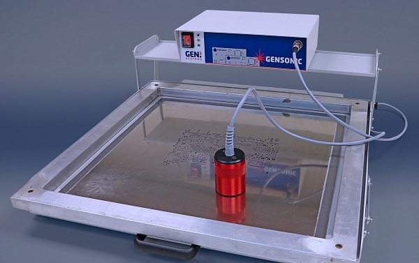
Effective cleaning of step-up stencils requires specialized techniques due to their varying thicknesses. Use ultrasonic cleaning systems with compatible solvents to remove paste residues from all zones. Manual wiping with lint-free cloths and approved cleaning agents can target stubborn deposits in transition areas. Establishing a cleaning frequency based on production volume prevents buildup and extends stencil lifespan. Refer to IPC-7525B for best practices in stencil maintenance.
Troubleshooting Insights for Electrical Engineers
When troubleshooting step-up stencil issues, a systematic approach is crucial. Start by isolating the defect type through visual inspection or automated optical tools. For instance, if solder bridging appears near step-up zones, review the stencil design and printing parameters before adjusting paste volume. Documenting each print run’s settings, including squeegee speed and pressure, helps identify patterns in recurring defects. Collaboration between design and assembly teams ensures that stencil specifications align with PCB layouts. Testing small batches after parameter adjustments can validate solutions without risking large-scale production errors. This iterative process, grounded in practical experience, minimizes downtime and enhances assembly quality.
Conclusion
Step-up stencil printing is a powerful technique for accommodating diverse component requirements in PCB assembly, but it comes with unique challenges. Issues like step-up stencil solder bridging, insufficient solder, paste smearing, misalignment, and cleaning difficulties can disrupt production if not addressed. By understanding the technical principles behind these problems and applying practical solutions, electrical engineers can optimize the printing process for consistent results. Adhering to industry standards and maintaining rigorous process controls are essential steps in achieving defect-free assemblies. With careful attention to design and execution, step-up stencil printing can significantly enhance the reliability of complex electronic boards.
FAQs
Q1: What causes step-up stencil solder bridging in PCB assembly?
A1: Step-up stencil solder bridging often results from excessive solder paste deposition in thicker stencil zones near fine-pitch components. Incorrect aperture sizes or high squeegee pressure can push excess paste between pads, creating shorts. Adjusting stencil design per industry guidelines and optimizing printing parameters can prevent this defect. Regular inspection helps catch issues early.
Q2: How can I fix step-up stencil insufficient solder on larger pads?
A2: Insufficient solder in step-up areas may stem from poor paste release or inadequate aperture dimensions. Ensure stencil thickness and aperture ratios meet component needs as per standards like IPC-7525B. Fine-tune squeegee pressure and test paste formulations for better transfer. Small batch testing validates adjustments before full production.
Q3: Why does step-up stencil paste smearing occur during printing?
A3: Step-up stencil paste smearing typically occurs due to excessive squeegee pressure or stencil surface contamination. This spreads paste beyond intended areas, risking defects. Maintain optimal pressure settings and keep the stencil clean using proper solvents. A controlled printing environment further reduces contamination risks during assembly.
Q4: What are best practices for step-up stencil cleaning in SMT processes?
A4: Cleaning step-up stencils requires addressing varying thicknesses. Use ultrasonic systems with compatible solvents to remove residues from all zones. Manual cleaning with lint-free cloths targets stubborn deposits. Follow a regular schedule based on production volume and adhere to maintenance guidelines in IPC-7525B for consistent stencil performance.
References
IPC-7525B - Stencil Design Guidelines. IPC, 2011.
IPC-A-600K - Acceptability of Printed Boards. IPC, 2020.


