Introduction
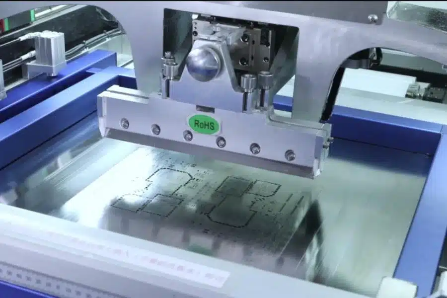
Step stencils play a critical role in surface mount technology assembly, enabling precise solder paste deposition on boards with components of varying heights. These multi-level stencils allow thicker paste volumes for larger parts like QFNs or BGAs while maintaining finer deposits for smaller chips, optimizing reflow solder joint formation. However, issues such as solder paste bridging, insufficient solder, stencil alignment errors, and inadequate stencil cleaning frequently disrupt SMT assembly troubleshooting efforts. Engineers often encounter yield losses from these defects, which can stem from design, printing, or maintenance oversights. This practical guide provides targeted strategies to identify and resolve common step stencil problems, drawing on established engineering principles to enhance assembly reliability.
What Are Step Stencils and Why Do They Matter?
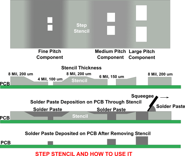
Step stencils feature multiple thickness levels etched or electroformed into a single foil, typically stainless steel or nickel, to accommodate diverse component standoffs on the same PCB. Thicker sections, often 0.15 mm or more, deliver higher solder paste volumes to pads under tall-profile devices, preventing defects like insufficient solder during reflow. Thinner areas, around 0.1 mm, ensure controlled deposition for fine-pitch parts, reducing risks of solder paste bridging between closely spaced pads. This design versatility is essential for modern high-density boards where uniform stencil thickness would compromise joint quality. Without proper step stencil implementation, SMT assembly troubleshooting becomes routine, as mismatched paste heights lead to inconsistent reflow profiles and reliability failures. Adhering to guidelines like those in IPC-7525B ensures step stencils support efficient production scaling.
Understanding the Causes of Step Stencil Problems
Step stencil issues often trace back to fundamental printing mechanics, where solder paste transfer depends on stencil thickness, aperture geometry, and board-stencil contact. Solder paste bridging occurs when excess paste volume from thick step areas smears across adjacent pads, especially if apertures lack adequate keep-out zones between thickness transitions. Insufficient solder paste deposits arise from poor release in thin sections, caused by residue buildup or overly aggressive squeegee pressure that compacts the paste. Stencil alignment deviations, even by microns, shift paste patterns relative to pads, exacerbating both bridging and starvation defects during SMT assembly troubleshooting. Inadequate stencil cleaning compounds these by leaving dried paste particles that alter aperture dimensions over time. Engineers must analyze these interconnected causes systematically to pinpoint root failures.
Poor aperture design in step stencils frequently triggers solder paste bridging, as oversized openings in thicker zones fail to contain paste flow during printing. IPC-7525B outlines specific rules for step-down distances and aperture reductions to mitigate this, emphasizing proportional setbacks from thickness changes. Misalignment compounds the issue, where fiducial mark offsets or warped boards prevent parallel stencil-to-PCB contact, leading to skewed deposits. Insufficient solder often links to thin-step adhesion, where paste clings to stencil walls due to surface tension or contamination, resulting in voids post-reflow. Stencil cleaning lapses allow oxidized residues to form, further hindering clean release and promoting inconsistent transfer. Routine process audits reveal these patterns, guiding targeted interventions.
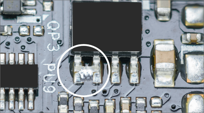
Solder Paste Bridging: Root Causes and Identification
Solder paste bridging manifests as unintended connections between pads, immediately visible under inspection and a top SMT assembly troubleshooting concern. Primary causes include excessive paste height in step stencil thick areas, where high-volume deposits slump during snap-off, forming bridges on fine-pitch arrays. Aperture walls with burrs or rounded edges from fabrication trap paste, delaying release and allowing lateral spread. High squeegee speeds or pressures push paste beyond pad boundaries, particularly if alignment tolerances exceed process windows. Environmental factors like high humidity thicken paste viscosity, amplifying bridging in step transitions. Visual and automated solder paste inspection tools confirm bridging by measuring deposit height and bridging length against IPC-A-610 criteria for acceptable joints.
To differentiate bridging from other defects, engineers check print transfer efficiency, typically targeting 75-125% of pad area coverage. Step stencil-specific bridging clusters near thickness changes, where paste from adjacent thick apertures contaminates thin zones. Process data loggers capture squeegee force and speed variations correlating with defect spikes. Board warpage exacerbates this by tilting the stencil plane, unevenly distributing paste pressure. Addressing these requires holistic process mapping before isolated fixes.
Insufficient Solder: Mechanisms and Prevention Insights
Insufficient solder appears as low-volume deposits or reflow voids, weakening joint strength and failing reliability tests. In step stencils, thin areas prone to this suffer from incomplete paste release, often due to high aspect ratios where aperture depth exceeds width by more than 1.5:1. Paste formulation mismatches, like low metal content, reduce slump resistance but hinder clean lift-off from stencil walls. Over-cleaning thins apertures microscopically, dropping transfer volumes below reflow thresholds. Stencil alignment shifts starve outer pad edges, mimicking insufficient solder patterns. SMT assembly troubleshooting logs highlight these through volume histograms from SPI systems.
Engineers quantify insufficient solder by averaging deposit heights across component types, flagging variances exceeding 20%. Step stencil calibration ensures thin zones match component lead coplanarity specs. Paste shear-thinning properties demand balanced printing parameters to avoid compaction.
Stencil Alignment Challenges in Step Printing
Stencil alignment precision, critical for step stencils, relies on fiducials and vision systems to achieve sub-25 micron registration. Misalignment stems from loose fixtures, thermal expansion mismatches between stencil and PCB, or operator errors in setup. This shifts paste centroids, causing bridging on one side and insufficient solder on the other. High-mix production amplifies risks as frequent changeovers disrupt zero-point calibration. Warped substrates compound offsets, with bow exceeding 0.75% of panel dimension per IPC standards. Troubleshooting involves overlaying SPI images with design data to visualize shifts.
Stencil Cleaning: A Frequent Oversight
Stencil cleaning prevents residue accumulation that degrades aperture fidelity over thousands of prints. Manual wiping leaves smears, while automated under-stencil cleaners using solvent or vacuum fail if cycles mismatch paste type. Dried paste hardens in step ledges, blocking thin apertures and causing inconsistent release. Over-reliance on wipe-only methods ignores nano-coatings that require specific cleaners. IPC-7526 provides frameworks for cleaning validation, stressing residue-free verification post-cycle. Regular microscope checks detect early degradation.
Practical Solutions and Best Practices
Mitigate solder paste bridging by optimizing step stencil apertures per IPC-7525B, applying 5-10% reductions in thick zones and ensuring keep-out rules around steps. Implement SPI for real-time volume and bridging detection, adjusting squeegee speed downward for high-pitch areas. For insufficient solder, select type-4 or finer paste and validate release with laser-cut stencils featuring trapezoidal walls. Stencil alignment best practices include dual-camera vision systems and automated fiducial teaching, targeting <15 micron offsets. Stencil cleaning protocols should combine vacuum, spray, and dry wipe in sequence, with daily audits using gloss meters for surface integrity. Process DOE isolates variables, like pressure vs. speed trade-offs, boosting first-pass yields.
| Problem | Key Causes | Troubleshooting Steps | Best Practice Fixes |
|---|---|---|---|
| Solder Paste Bridging | Excess thick-area paste, poor snap-off | SPI bridging scan, aperture inspection | Aperture reduction, slower squeegee |
| Insufficient Solder | Thin-zone adhesion, high aspect ratio | Volume profiling, wall residue check | Finer mesh paste, nano-coated stencil |
| Stencil Alignment | Fiducial offset, warpage | Overlay analysis, bow measurement | Vision auto-align, substrate flattening |
| Stencil Cleaning | Residue buildup, improper cycle | Microscope audit, contact angle test | Automated multi-stage cleaning |
Integrate these into a preventive maintenance loop: daily alignment verification, post-shift cleaning, and weekly stencil tension checks. Train operators on paste-in-aperture ratios and step-specific parameters. For high-volume runs, consider framed stencils with tensioners to maintain flatness.
SMT Assembly Troubleshooting Case Insights
Consider a scenario where a step stencil board showed 15% bridging on QFN sites amid 5% insufficient solder elsewhere. Root cause analysis via SPI revealed 30-micron alignment drift and residue in thin steps. Correcting fiducials and extending cleaning cycles dropped defects to under 1%. Another case involved fine-pitch bridging from thick-step overflow; redesigning keep-outs per IPC guidelines resolved it. These highlight data-driven iteration over trial-and-error.
Conclusion
Troubleshooting step stencil problems demands attention to solder paste bridging, insufficient solder, stencil alignment, and stencil cleaning interplays. By grounding practices in IPC-7525B and IPC-A-610 frameworks, engineers achieve robust SMT assembly troubleshooting outcomes. Proactive design reviews, precise printing parameters, and rigorous maintenance form the backbone of defect-free production. Implementing these strategies not only cuts rework but elevates overall assembly yields and reliability. Regular process monitoring ensures sustained performance across production scales.
FAQs
Q1: How do you prevent solder paste bridging with step stencils?
A1: Solder paste bridging in step stencils often results from excess volume in thick areas or misalignment. Optimize aperture sizes with reductions in high-paste zones and ensure keep-out distances around steps follow IPC-7525B guidelines. Use SPI to monitor deposit shapes and adjust squeegee pressure for cleaner snap-off. Automated alignment systems maintain registration below 20 microns, minimizing smear risks during SMT assembly troubleshooting. Consistent stencil cleaning prevents residue-induced bridging.
Q2: What causes insufficient solder in SMT stencil printing?
A2: Insufficient solder typically stems from poor paste release in thin stencil sections or overly thin apertures. High aspect ratios trap paste against walls, while contamination hinders transfer. Validate with volume measurements targeting 100-120% pad coverage and select shear-thinning pastes suited to step designs. Enhance release via electropolished surfaces and balanced printing speeds. This addresses common SMT assembly troubleshooting pain points effectively.
Q3: Why is stencil alignment critical for step stencils?
A3: Stencil alignment ensures paste lands precisely on pads, avoiding bridging or starvation in multi-level designs. Deviations amplify at thickness transitions, skewing deposits. Employ fiducial-based vision systems for sub-micron accuracy and check board flatness pre-print. Regular calibration counters thermal drifts. Proper alignment streamlines SMT assembly troubleshooting by stabilizing transfer efficiency.
Q4: Best practices for stencil cleaning in high-volume production?
A4: Stencil cleaning maintains aperture integrity, preventing buildup that causes inconsistent paste release. Use automated under-stencil systems with solvent spray, vacuum, and wipe sequences tailored to paste type. Audit daily with residue tests and replace media proactively. IPC-7526 insights guide frequency to match print counts. This sustains quality in step stencil applications.
References
IPC-7525B — Stencil Design Guidelines. IPC, 2011
IPC-A-610G — Acceptability of Electronic Assemblies. IPC, 2017
IPC-7526 — Stencil and Misprinted Board Cleaning Handbook. IPC, 2007


