Introduction
Wave soldering remains a cornerstone process in through-hole PCB assembly, where molten solder flows over the board underside to form reliable joints. Electric engineers often encounter defects that compromise electrical performance and reliability, such as wave soldering bridging, wave soldering insufficient solder, wave soldering icicles, and wave soldering pinholes. These issues can lead to shorts, weak connections, or voids that fail under thermal stress or vibration. Understanding their root causes allows for targeted troubleshooting, reducing rework and improving yield. This practical guide draws on engineering principles to diagnose and resolve these defects systematically. By addressing them proactively, engineers ensure assemblies meet performance demands in demanding applications.
Understanding Wave Soldering and Its Challenges
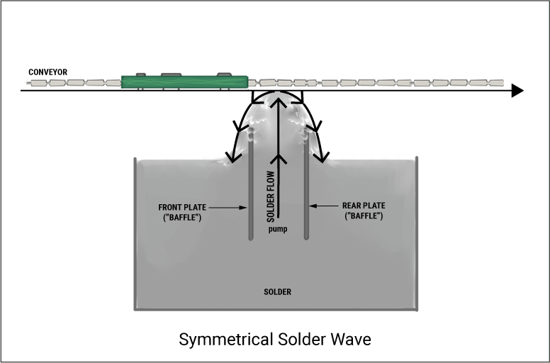
Wave soldering involves three main stages: flux application, preheating, and solder wave contact. Flux cleans oxides and promotes wetting, preheating activates flux and prevents thermal shock, while the solder wave forms fillets on leads and pads. Defects arise from imbalances in these stages, influenced by parameters like conveyor speed, flux quantity, preheat temperature, and wave height. For electric engineers, these problems matter because they directly affect signal integrity, power delivery, and long-term reliability in circuits. Industry standards like J-STD-001 define soldering requirements to classify acceptable joints, emphasizing the need for consistent process control. Mastering these fundamentals enables precise defect isolation during production runs.
Wave Soldering Bridging: Causes and Diagnosis
Wave soldering bridging occurs when excess solder connects adjacent pins or pads, creating unintended shorts. Common causes include over-application of flux, which enhances solder flow excessively, or turbulent wave dynamics that splash solder between closely spaced leads. High solder pot temperature can lower viscosity, exacerbating bridging on fine-pitch components, while inadequate masking on non-solder areas allows solder migration. Poor board design, such as insufficient spacing per IPC guidelines, amplifies the risk during the soldering phase. Engineers diagnose bridging visually under magnification, confirming electrical continuity tests reveal shorts. Process logs, including flux density and wave contact time, help pinpoint deviations.
To troubleshoot, first inspect fluxer nozzles for uniform spray patterns and adjust volume to recommended levels, typically avoiding puddling. Reduce wave height or smooth turbulence with proper weir design to control solder volume. Preheating boards to flux activation temperature, around 100-120°C, improves wetting without excess flow. Masking tapes or solder resists must cover exposed copper fully. Implementing these steps often resolves bridging, with verification through post-solder cleaning and inspection.
Wave Soldering Insufficient Solder: Identifying and Fixing Shortfalls
Wave soldering insufficient solder manifests as incomplete fillet formation or dry joints, where pads lack proper coverage. This defect stems from inadequate hole plating thickness, which hinders capillary action, or insufficient preheat that fails to expand plated holes for solder entry. Excessive conveyor speed shortens dwell time over the wave, starving joints of solder, while weak flux activity leaves oxides intact, repelling molten solder. Engineers spot this via X-ray or cross-section analysis, noting thin intermetallic layers or unfilled barrels. Consistent documentation of preheat profiles and speed settings aids diagnosis.
According to IPC-A-610 acceptability criteria, insufficient solder joints fall outside Class 2 and 3 requirements due to reliability risks. Solutions start with verifying copper plating thickness meets specifications, ensuring robust barrel walls for solder wicking. Optimize preheat to achieve uniform board temperature, promoting flux efficacy and hole expansion. Slow conveyor speed to extend wave contact to 3-5 seconds, balancing with flux to avoid other defects. Post-process fillet inspection confirms improvements, minimizing open joints.
Wave Soldering Icicles: Mechanisms and Prevention Strategies
Wave soldering icicles are elongated solder spikes protruding from joints, often due to dross accumulation on the wave surface or improper board angle. Dross, oxidized solder particles, adheres to leads during contact, solidifying as spikes upon withdrawal. Steep board angles prolong dripping, while low flux coverage fails to shield leads from oxidation mid-process. High solder temperature accelerates dross formation, compounding the issue on vertical tails. Diagnosis involves microscopic examination for spike length exceeding heel height and process parameter review.
Preventing icicles requires regular skimming of the solder pot to remove dross, maintaining a clean wave. Adjust board tilt to 5-10 degrees for optimal drainage without excess hang-up. Increase flux application for better protection, ensuring it reaches pin heels. Nitrogen blanketing over the wave reduces oxidation, minimizing dross altogether. These practices align with J-STD-001 soldering standards, yielding smoother fillets.
Wave Soldering Pinholes: Root Causes and Resolution
Wave soldering pinholes appear as small voids or gas bubbles trapped in solidified solder, compromising joint strength. Primary causes trace to flux outgassing during reflow, where volatile residues release hydrogen or moisture under heat. Contaminated solder pots introduce impurities that evolve gases, while rapid cooling traps them before escape. Inadequate preheating leaves moisture in board laminates, vaporizing on the wave. Engineers detect pinholes via dye penetrant testing or microscopy, quantifying density against acceptability thresholds.
Addressing pinholes demands low-residue, no-clean flux selection to minimize volatiles. Preheat boards thoroughly to drive off moisture, targeting laminate temperatures per process specs. Filter solder regularly to eliminate oxides and contaminants. Extend cooling zones for gradual solidification, allowing gas escape. Cross-verification with thermal profiling ensures parameter stability.
Best Practices for Wave Soldering Process Optimization
Holistic process control prevents multiple defects simultaneously. Establish statistical process control charts for key variables like flux weight, preheat delta-T, and wave height. Train operators on daily maintenance, including pot skimming and nozzle calibration. Board design collaboration ensures adequate pad sizes and lead trims compliant with standards. Fixturing minimizes warpage, maintaining consistent wave contact. Inline AOI systems catch defects early, feeding data back for adjustments.
For electric engineers, integrating these into workflows boosts first-pass yield. Periodic audits against IPC-A-610 verify compliance across classes.
Conclusion
Troubleshooting wave soldering defects like bridging, insufficient solder, icicles, and pinholes requires a methodical approach rooted in process understanding. By diagnosing causes through inspection and logs, then applying targeted fixes like flux optimization and preheat control, engineers achieve reliable assemblies. Standards such as J-STD-001 and IPC-A-610 provide benchmarks for excellence. Consistent application of best practices not only resolves issues but elevates overall production quality. Electric engineers equipped with this guide can minimize downtime and enhance circuit performance effectively.
FAQs
Q1: What causes wave soldering bridging and how can it be prevented?
A1: Wave soldering bridging results from excess flux, turbulent waves, or inadequate masking, leading to solder shorts between pins. Prevent it by calibrating flux spray for uniformity, reducing wave height to control flow, and ensuring robust solder resist coverage. Preheating boards properly activates flux without over-wetting. Regular process monitoring per J-STD-001 standards maintains spacing integrity. These steps typically eliminate bridging in production.
Q2: How do you fix wave soldering insufficient solder on through-hole joints?
A2: Wave soldering insufficient solder arises from fast conveyor speeds, poor plating, or weak flux. Resolve by slowing speed for 3-5 second dwell, verifying plating thickness, and optimizing preheat for hole expansion. Flux must clean oxides effectively for capillary action. IPC-A-610 criteria guide fillet acceptance. Inspection post-adjustment confirms full coverage.
Q3: Why do wave soldering icicles form and what is the best prevention?
A3: Wave soldering icicles form from dross on the wave, steep angles, or insufficient flux, creating spikes. Prevent by skimming pots daily, tilting boards 5-10 degrees, and enhancing flux protection. Nitrogen atmospheres cut oxidation. This aligns with soldering best practices, smoothing joints.
Q4: What are the main triggers for wave soldering pinholes?
A4: Wave soldering pinholes stem from flux outgassing, moisture in boards, or solder impurities trapping gas. Mitigate with low-volatile flux, thorough preheating, and filtered pots. Gradual cooling aids escape. Dye testing verifies resolution, ensuring void-free joints.
References
J-STD-001H — Requirements for Soldered Electrical and Electronic Assemblies. IPC, 2018
IPC-A-610H — Acceptability of Electronic Assemblies. IPC, 2019


